- 您现在的位置:买卖IC网 > PDF目录29137 > MPC9893FAR2 (INTEGRATED DEVICE TECHNOLOGY INC) 9893 SERIES, PLL BASED CLOCK DRIVER, 12 TRUE OUTPUT(S), 0 INVERTED OUTPUT(S), PQFP48 PDF资料下载
参数资料
| 型号: | MPC9893FAR2 |
| 厂商: | INTEGRATED DEVICE TECHNOLOGY INC |
| 元件分类: | 时钟及定时 |
| 英文描述: | 9893 SERIES, PLL BASED CLOCK DRIVER, 12 TRUE OUTPUT(S), 0 INVERTED OUTPUT(S), PQFP48 |
| 封装: | 7 X 7 MM, LQFP-48 |
| 文件页数: | 10/16页 |
| 文件大小: | 285K |
| 代理商: | MPC9893FAR2 |
MPC9893
TIMING SOLUTIONS
3
MOTOROLA
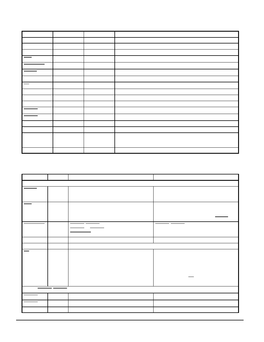
Table 1: PIN CONFIGURATION
Pin
I/O
Type
Function
CLK0, CLK1
Input
LVCMOS
PLL reference clock inputs
FB
Input
LVCMOS
PLL feedback signal input, connect directly to QFB output
REF_SEL
Input
LVCMOS
Selects the primary reference clock
MAN/A
Input
LVCMOS
Selects automatic switch mode or manual reference clock selection
ALARM_RST
Input
LVCMOS
Reset of alarm flags and selected reference clock
PLL_EN
Input
LVCMOS
Select PLL or static test mode
FSEL[0:3]
Input
LVCMOS
Clock frequency selection and configuration of clock divider modes
OE/MR
Input
LVCMOS
Output enable/disable and device reset
QA[0:5]
Output
LVCMOS
Bank A clock outputs
QB[0:5]
Output
LVCMOS
Bank B clock outputs
QFB
Output
LVCMOS
Clock feedback output. QFB must be connected to FB for correct operation
ALARM0
Output
LVCMOS
Indicates clock failure on CLK0
ALARM1
Output
LVCMOS
Indicates clock failure on CLK1
CLK_IND
Output
LVCMOS
Indicates currently selected input reference clock
GND
Supply
Ground
Negative power supply
VCC_PLL
Supply
VCC
Positive power supply for the PLL (analog power supply). It is recommended to
use an external RC filter for the analog power supply pin VCC_PLL. Please see
the application section for details.
VCC
Supply
VCC
Positive power supply for I/O and core
Table 2: FUNCTION TABLE
Control
Default
0
1
Inputs
PLL_EN
0
PLL enabled. The input to output frequency
relationship is that according to Table 3 if the PLL is
frequency locked.
PLL bypassed and IDCS disabled. The VCO output is
replaced by the reference clock signal fref. The
MPC9893 is in manual mode.
MAN/A
1
Manual clock switch mode. IDCS disabled.Clock
failure detection and output flags ALARM0, ALARM1,
CLK_IND are enabled.
Automatic clock switch mode. IDCS enabled.Clock
failure detection and output flags ALARM0, ALARM1,
CLK_IND are enabled. IDCS overrides REF_SEL on
a clock failure. IDCS operation requires PLL_EN =0.
ALARM_RST
1
ALARM0,ALARM1 and CLK_IND flags are reset:
ALARM0=H, ALARM1=H and CLK_IND=REF_SEL.
ALARM_RST is an one-shot function.
ALARM0,ALARM1 and CLK_IND active
REF_SEL
0
Selects CLK0 as the primary clock source
Selects CLK1 as the secondary clock source
FSEL[0:3]
0000
See Following Table
OE/MR
0
Outputs enabled (active)
Outputs disabled (high impedance tristate), reset of
data generators and output dividers. The MPC9893
requires reset at power-up and after any loss of PLL
lock. Loss of PLL lock may occur when the external
feedback path is interrupted. The length of the reset
pulse should be greater than two reference clock
cycles (CLK0,1). MR/OE does not tristate the QFB
output.
Outputs (ALARM0,ALARM1, CLK_IND are valid if PLL is locked)
ALARM0
CLK0 failure
ALARM1
CLK1 failure
CLK_IND
CLK0 is the reference clock
CLK1 is the reference clock
相关PDF资料 |
PDF描述 |
|---|---|
| MPC991FAR2 | PLL BASED CLOCK DRIVER, 13 TRUE OUTPUT(S), 0 INVERTED OUTPUT(S), PQFP52 |
| MPC991FAR2 | PLL BASED CLOCK DRIVER, 13 TRUE OUTPUT(S), 0 INVERTED OUTPUT(S), PQFP52 |
| MPC993FA | 993 SERIES, PLL BASED CLOCK DRIVER, 5 TRUE OUTPUT(S), 0 INVERTED OUTPUT(S), PQFP32 |
| MPC9952FAR2 | PLL BASED CLOCK DRIVER, 11 TRUE OUTPUT(S), 0 INVERTED OUTPUT(S), PQFP32 |
| MPC9952FA | PLL BASED CLOCK DRIVER, 11 TRUE OUTPUT(S), 0 INVERTED OUTPUT(S), PQFP32 |
相关代理商/技术参数 |
参数描述 |
|---|---|
| MPC9894 | 制造商:未知厂家 制造商全称:未知厂家 功能描述:Quad Input Redundant IDCS Clock Generator |
| MPC9894VM | 制造商:IDT from Components Direct 功能描述:IDT MPC9894VM PLL - Trays 制造商:IDT 功能描述:IDT MPC9894VM PLL |
| MPC990 | 制造商:MOTOROLA 制造商全称:Motorola, Inc 功能描述:LOW VOLTAGE PLL CLOCK DRIVER |
| MPC990F18 F44A WAF | 制造商:Motorola Inc 功能描述: |
| MPC991 | 制造商:MOTOROLA 制造商全称:Motorola, Inc 功能描述:LOW VOLTAGE PLL CLOCK DRIVER |
发布紧急采购,3分钟左右您将得到回复。