- 您现在的位置:买卖IC网 > PDF目录29137 > MPC9893FAR2 (INTEGRATED DEVICE TECHNOLOGY INC) 9893 SERIES, PLL BASED CLOCK DRIVER, 12 TRUE OUTPUT(S), 0 INVERTED OUTPUT(S), PQFP48 PDF资料下载
参数资料
| 型号: | MPC9893FAR2 |
| 厂商: | INTEGRATED DEVICE TECHNOLOGY INC |
| 元件分类: | 时钟及定时 |
| 英文描述: | 9893 SERIES, PLL BASED CLOCK DRIVER, 12 TRUE OUTPUT(S), 0 INVERTED OUTPUT(S), PQFP48 |
| 封装: | 7 X 7 MM, LQFP-48 |
| 文件页数: | 13/16页 |
| 文件大小: | 285K |
| 代理商: | MPC9893FAR2 |
MPC9893
MOTOROLA
TIMING SOLUTIONS
6
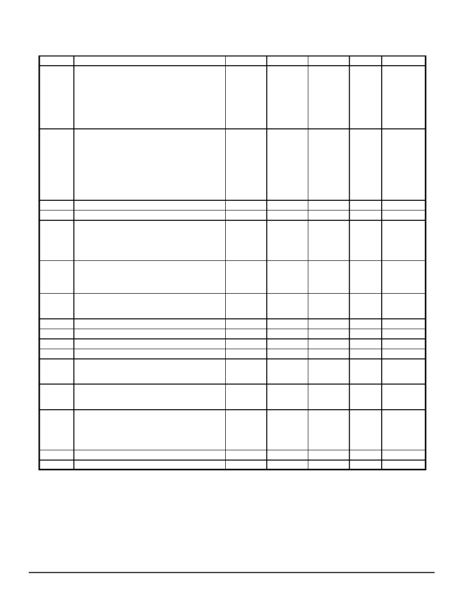
Table 8: AC CHARACTERISTICS (VCC =3.3V ± 5% or VCC =2.5V ± 5%, TA =--40° to 85°C)a
Symbol
Characteristics
Min
Typ
Max
Unit
Condition
fref
Input Frequency
FSEL= 000x
FSEL= 001x
FSEL= 010x
FSEL= 011x
FSEL= 100x
FSEL= 101x
FSEL= 110x
FSEL= 111x
15.0
30.0
40.0
30.0
60.0
15.0
30.0
60.0
25.0
50.0
66.6
50.0
100.0
12.5
50.0
100.0
MHz
PLL locked
fMAX
Maximum Output Frequency
FSEL= 000x
FSEL= 001x
FSEL= 010x
FSEL= 011x
FSEL= 100x
FSEL= 101x
FSEL= 110x
FSEL= 111x
60.0
30.0
60.0
7.5
15.0
30.0
200.0
100.0
200.0
25.0
50.0
100.0
MHz
PLL locked
frefDC
Reference Input Duty Cycle
40
60
%
tr, tf
CLK0, 1 Input Rise/Fall Time
1.0
ns
0.8to2.0V
t()
Propagation Delay (static phase offset, CLKx to FB)
VCC=3.3V±5% and FSEL[0:2]=111
VCC=3.3V±5%
VCC=2.5V±5% and FSEL[0:2]=111
VCC=2.5V±5%
--60
-200
-125
-400
+50
+100
+25
+100
ps
PLL locked
t
Rate of period change (phase slew rate)
QAx outputs
QBx outputs (FSEL=xxx0)
QBx outputs (FSEL=xxx1)
150
300
ps/cycle
Failover
switch
tsk(O)
Output-to-output Skewb
(within bank)
(bank-to-bank)
(any output to QFB)
50
100
125
ps
DCO
Output duty Cycle
45
50
55
%
tr,tf
Output Rise/Fall Time
0.1
1.0
ns
0.55 to 2.4V
tPLZ, HZ
Output Disable Time
10
ns
tPZL, LZ
Output Enable Time
10
ns
tJIT(CC)
Cycle-to-cycle jitterc
FSEL3=0
FSEL3=1
225
425
ps
See
applications
section
tJIT(PER)
Period Jitterc
FSEL3=0
FSEL3=1
150
250
ps
See
applications
section
tJIT()
I/O Phase Jitterd
FB=4: FSEL[0:2]=100 or 111
RMS (1 σ)
FB=6: FSEL[0:2]=010
RMS (1 σ)
FB=8: FSEL[0:2]=001, 011, or 110
RMS (1 σ)
FB=16: FSEL[0:2]=000 or 101
RMS (1 σ)
40
50
55
70
ps
See
applications
section
BW
PLL closed loop bandwidthe
FSEL=111x
0.8-4.0
MHz
tLOCK
Maximum PLL Lock Time
10
ms
a.
AC characteristics apply for parallel output termination of 50 to VTT.
b.
See application section for part-to-part skew calculation.
c.
Cycle-to-cycle and period jitter depend on the VCO frequency and output configuration. See the application section on page 9.
d.
I/O jitter depends on the VCO frequency and internal PLL feedback divider FB. See application section on page 8 and 9 for more
information and for the calculation for other confidence factors than 1σ.
e.
-3dB point of PLL transfer characteristics.
相关PDF资料 |
PDF描述 |
|---|---|
| MPC991FAR2 | PLL BASED CLOCK DRIVER, 13 TRUE OUTPUT(S), 0 INVERTED OUTPUT(S), PQFP52 |
| MPC991FAR2 | PLL BASED CLOCK DRIVER, 13 TRUE OUTPUT(S), 0 INVERTED OUTPUT(S), PQFP52 |
| MPC993FA | 993 SERIES, PLL BASED CLOCK DRIVER, 5 TRUE OUTPUT(S), 0 INVERTED OUTPUT(S), PQFP32 |
| MPC9952FAR2 | PLL BASED CLOCK DRIVER, 11 TRUE OUTPUT(S), 0 INVERTED OUTPUT(S), PQFP32 |
| MPC9952FA | PLL BASED CLOCK DRIVER, 11 TRUE OUTPUT(S), 0 INVERTED OUTPUT(S), PQFP32 |
相关代理商/技术参数 |
参数描述 |
|---|---|
| MPC9894 | 制造商:未知厂家 制造商全称:未知厂家 功能描述:Quad Input Redundant IDCS Clock Generator |
| MPC9894VM | 制造商:IDT from Components Direct 功能描述:IDT MPC9894VM PLL - Trays 制造商:IDT 功能描述:IDT MPC9894VM PLL |
| MPC990 | 制造商:MOTOROLA 制造商全称:Motorola, Inc 功能描述:LOW VOLTAGE PLL CLOCK DRIVER |
| MPC990F18 F44A WAF | 制造商:Motorola Inc 功能描述: |
| MPC991 | 制造商:MOTOROLA 制造商全称:Motorola, Inc 功能描述:LOW VOLTAGE PLL CLOCK DRIVER |
发布紧急采购,3分钟左右您将得到回复。