- 您现在的位置:买卖IC网 > PDF目录29137 > MPC9893FAR2 (INTEGRATED DEVICE TECHNOLOGY INC) 9893 SERIES, PLL BASED CLOCK DRIVER, 12 TRUE OUTPUT(S), 0 INVERTED OUTPUT(S), PQFP48 PDF资料下载
参数资料
| 型号: | MPC9893FAR2 |
| 厂商: | INTEGRATED DEVICE TECHNOLOGY INC |
| 元件分类: | 时钟及定时 |
| 英文描述: | 9893 SERIES, PLL BASED CLOCK DRIVER, 12 TRUE OUTPUT(S), 0 INVERTED OUTPUT(S), PQFP48 |
| 封装: | 7 X 7 MM, LQFP-48 |
| 文件页数: | 2/16页 |
| 文件大小: | 285K |
| 代理商: | MPC9893FAR2 |
MPC9893
MOTOROLA
TIMING SOLUTIONS
10
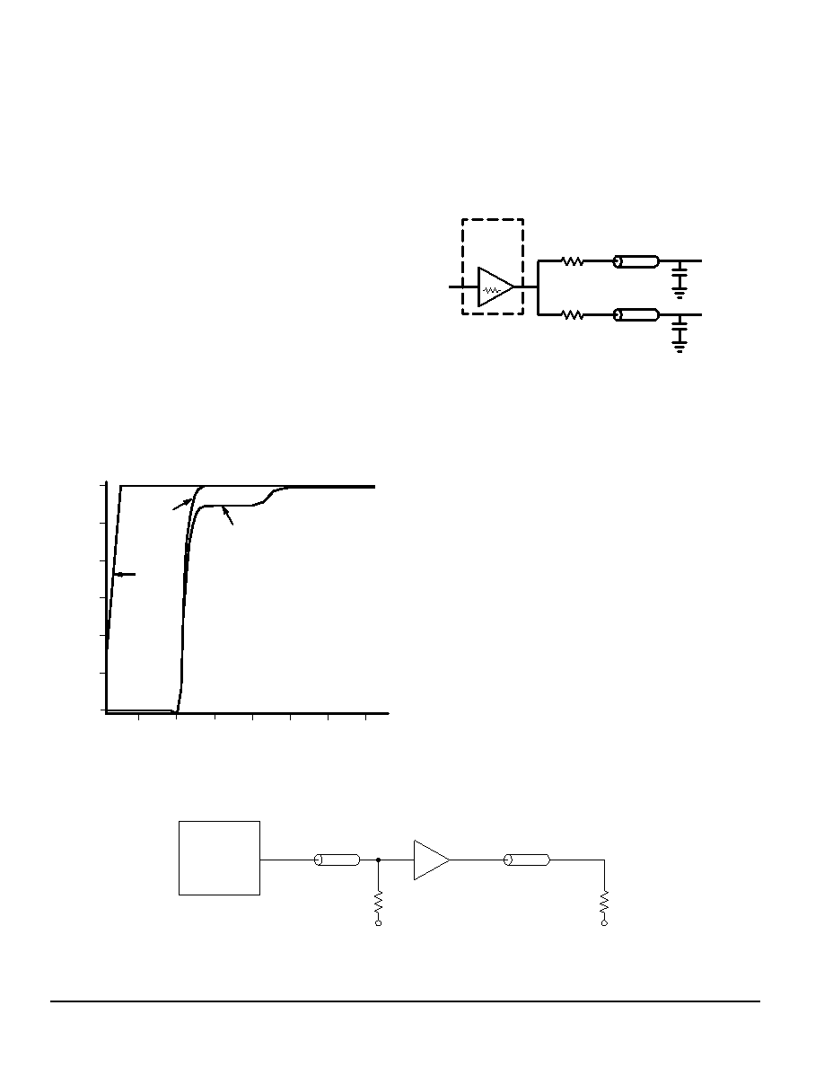
The waveform plots in Figure 9. “Single versus Dual Line
Termination Waveforms” show the simulation results of an
output driving a single line versus two lines. In both cases the
drive capability of the MPC9893 output buffer is more than
sufficient to drive 50 transmission lines on the incident
edge. Note from the delay measurements in the simulations a
delta of only 43ps exists between the two differently loaded
outputs. This suggests that the dual line driving need not be
used exclusively to maintain the tight output-to-output skew
of the MPC9893. The output waveform in Figure 9. “Single
versus Dual Line Termination Waveforms” shows a step in
the waveform, this step is caused by the impedance
mismatch seen looking into the driver. The parallel
combination of the 36 series resistor plus the output
impedance does not match the parallel combination of the
line impedances. The voltage wave launched down the two
lines will equal:
VL =VS (Z0 ÷ (RS+R0 +Z0))
Z0 =50 || 50
RS =36 || 36
R0 =14
VL =3.0 ( 25 ÷ (18+17+25)
= 1.31V
At the load end the voltage will double, due to the near
unity reflection coefficient, to 2.6V. It will then increment
towards the quiescent 3.0V in steps separated by one round
trip delay (in this case 4.0ns).
Figure 9. Single versus Dual Waveforms
TIME (nS)
VOL
TAGE
(V)
3.0
2.5
2.0
1.5
1.0
0.5
0
246
8
10
12
14
OutB
tD = 3.9386
OutA
tD = 3.8956
In
Since this step is well above the threshold region it will not
cause any false clock triggering, however designers may be
uncomfortable with unwanted reflections on the line. To better
match the impedances when driving multiple lines the
situation in Figure 10. “Optimized Dual Line Termination”
should be used. In this case the series terminating resistors
are reduced such that when the parallel combination is added
to the output buffer impedance the line impedance is perfectly
matched.
Figure 10. Optimized Dual Line Termination
14
MPC9893
OUTPUT
BUFFER
RS =22
ZO =50
RS =22
ZO =50
14 +22 k 22 =50 k 50
25 =25
Figure 11. CLK0, CLK1 MPC9893 AC test reference for Vcc =3.3Vand Vcc =2.5V
Pulse
Generator
Z= 50
RT =50
ZO =50
RT =50
ZO =50
MPC9893 DUT
VTT
相关PDF资料 |
PDF描述 |
|---|---|
| MPC991FAR2 | PLL BASED CLOCK DRIVER, 13 TRUE OUTPUT(S), 0 INVERTED OUTPUT(S), PQFP52 |
| MPC991FAR2 | PLL BASED CLOCK DRIVER, 13 TRUE OUTPUT(S), 0 INVERTED OUTPUT(S), PQFP52 |
| MPC993FA | 993 SERIES, PLL BASED CLOCK DRIVER, 5 TRUE OUTPUT(S), 0 INVERTED OUTPUT(S), PQFP32 |
| MPC9952FAR2 | PLL BASED CLOCK DRIVER, 11 TRUE OUTPUT(S), 0 INVERTED OUTPUT(S), PQFP32 |
| MPC9952FA | PLL BASED CLOCK DRIVER, 11 TRUE OUTPUT(S), 0 INVERTED OUTPUT(S), PQFP32 |
相关代理商/技术参数 |
参数描述 |
|---|---|
| MPC9894 | 制造商:未知厂家 制造商全称:未知厂家 功能描述:Quad Input Redundant IDCS Clock Generator |
| MPC9894VM | 制造商:IDT from Components Direct 功能描述:IDT MPC9894VM PLL - Trays 制造商:IDT 功能描述:IDT MPC9894VM PLL |
| MPC990 | 制造商:MOTOROLA 制造商全称:Motorola, Inc 功能描述:LOW VOLTAGE PLL CLOCK DRIVER |
| MPC990F18 F44A WAF | 制造商:Motorola Inc 功能描述: |
| MPC991 | 制造商:MOTOROLA 制造商全称:Motorola, Inc 功能描述:LOW VOLTAGE PLL CLOCK DRIVER |
发布紧急采购,3分钟左右您将得到回复。