- 您现在的位置:买卖IC网 > PDF目录29137 > MPC9893FAR2 (INTEGRATED DEVICE TECHNOLOGY INC) 9893 SERIES, PLL BASED CLOCK DRIVER, 12 TRUE OUTPUT(S), 0 INVERTED OUTPUT(S), PQFP48 PDF资料下载
参数资料
| 型号: | MPC9893FAR2 |
| 厂商: | INTEGRATED DEVICE TECHNOLOGY INC |
| 元件分类: | 时钟及定时 |
| 英文描述: | 9893 SERIES, PLL BASED CLOCK DRIVER, 12 TRUE OUTPUT(S), 0 INVERTED OUTPUT(S), PQFP48 |
| 封装: | 7 X 7 MM, LQFP-48 |
| 文件页数: | 16/16页 |
| 文件大小: | 285K |
| 代理商: | MPC9893FAR2 |
MPC9893
TIMING SOLUTIONS
9
MOTOROLA
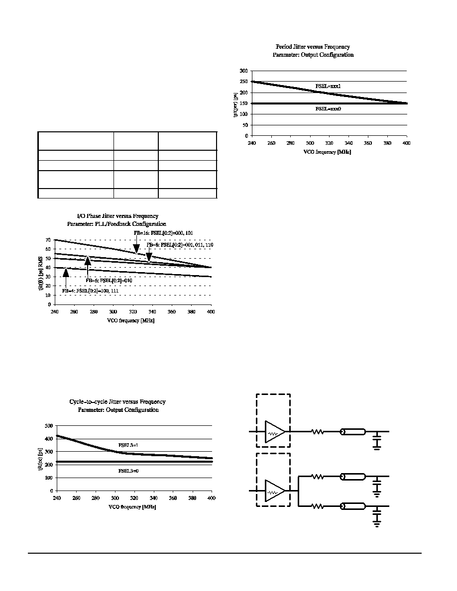
feedback divider result in lower I/O jitter than the jitter limits in
the AC characterisitics (table 8 on page 6). When calculating
the part--to--part skew, Table 11 “Internal VCO frequency
fVCO”
should be used to determine the actual VCO
frequency, then use Figure 5 “Max. I/O Phase Jitter versus
VCO Frequency” to determine the maximum I/O jitter for the
specific VCO frequency and divider configuration. In above
example calculation, the internal VCO frequency of 400 MHz
corresponds to a maximum I/O jitter of 30 ps (RMS).
Table 11: Internal VCO frequency fVCO
MPC9893
Configuration
fVCO
PLL feedback
divider FB
M1H, M12H, M2H, M22H
4* fref
4
M3, M32
6* fref
6
M1M, M12M, M2M,
M22M, M4, M42
8* fref
8
M1L, M12L, M8, M82
16 * fref
16
Figure 5. Max. I/O Phase Jitter versus VCO Frequency
The cycle--to--cycle jitter and period jitter of the MPC9893
depend on the output configuration and on the frequency of
the internal VCO. Using the outputs of bank A and bank B at
the same frequency (FSEL3=0) results in a lower jitter than
the split output frequency configuration (FSEL3=1). The jitter
also decreases with an increasing internal VCO frequency.
Figures 4 to 6 represent the maximum jitter of the MPC9893.
Figure 6. Max. Cycle--to--Cycle Jitter versus VCO
Frequency
Figure 7. Max. Period Jitter versus VCO Frequency
Driving Transmission Lines
The MPC9893 clock driver was designed to drive high
speed signals in a terminated transmission line environment.
To provide the optimum flexibility to the user the output
drivers were designed to exhibit the lowest impedance
possible. With an output impedance of less than 20 the
drivers can drive either parallel or series terminated
transmission lines. For more information on transmission
lines the reader is referred to Motorola application note
AN1091. In most high performance clock networks
point-to-point distribution of signals is the method of choice.
In a point-to-point scheme either series terminated or parallel
terminated transmission lines can be used. The parallel
technique terminates the signal at the end of the line with a
50 resistance to VCC÷2.
This technique draws a fairly high level of DC current and
thus only a single terminated line can be driven by each
output of the MPC9893 clock driver. For the series terminated
case however there is no DC current draw, thus the outputs
can drive multiple series terminated lines. Figure 8. “Single
versus Dual Transmission Lines” illustrates an output driving
a single series terminated line versus two series terminated
lines in parallel. When taken to its extreme the fanout of the
MPC9893 clock driver is effectively doubled due to its
capability to drive multiple lines.
Figure 8. Single versus Dual Transmission Lines
14
IN
MPC9893
OUTPUT
BUFFER
RS =36
ZO =50
OutA
14
IN
MPC9893
OUTPUT
BUFFER
RS =36
ZO =50
OutB0
RS =36
ZO =50
OutB1
相关PDF资料 |
PDF描述 |
|---|---|
| MPC991FAR2 | PLL BASED CLOCK DRIVER, 13 TRUE OUTPUT(S), 0 INVERTED OUTPUT(S), PQFP52 |
| MPC991FAR2 | PLL BASED CLOCK DRIVER, 13 TRUE OUTPUT(S), 0 INVERTED OUTPUT(S), PQFP52 |
| MPC993FA | 993 SERIES, PLL BASED CLOCK DRIVER, 5 TRUE OUTPUT(S), 0 INVERTED OUTPUT(S), PQFP32 |
| MPC9952FAR2 | PLL BASED CLOCK DRIVER, 11 TRUE OUTPUT(S), 0 INVERTED OUTPUT(S), PQFP32 |
| MPC9952FA | PLL BASED CLOCK DRIVER, 11 TRUE OUTPUT(S), 0 INVERTED OUTPUT(S), PQFP32 |
相关代理商/技术参数 |
参数描述 |
|---|---|
| MPC9894 | 制造商:未知厂家 制造商全称:未知厂家 功能描述:Quad Input Redundant IDCS Clock Generator |
| MPC9894VM | 制造商:IDT from Components Direct 功能描述:IDT MPC9894VM PLL - Trays 制造商:IDT 功能描述:IDT MPC9894VM PLL |
| MPC990 | 制造商:MOTOROLA 制造商全称:Motorola, Inc 功能描述:LOW VOLTAGE PLL CLOCK DRIVER |
| MPC990F18 F44A WAF | 制造商:Motorola Inc 功能描述: |
| MPC991 | 制造商:MOTOROLA 制造商全称:Motorola, Inc 功能描述:LOW VOLTAGE PLL CLOCK DRIVER |
发布紧急采购,3分钟左右您将得到回复。