- 您现在的位置:买卖IC网 > PDF目录98044 > MSC8144E (FREESCALE SEMICONDUCTOR INC) 0-BIT, 150 MHz, OTHER DSP, PBGA783 PDF资料下载
参数资料
| 型号: | MSC8144E |
| 厂商: | FREESCALE SEMICONDUCTOR INC |
| 元件分类: | 数字信号处理 |
| 英文描述: | 0-BIT, 150 MHz, OTHER DSP, PBGA783 |
| 封装: | 29 X 29 MM, LEAD FREE, PLASTIC, FCPBGA-783 |
| 文件页数: | 24/80页 |
| 文件大小: | 2284K |
| 代理商: | MSC8144E |
第1页第2页第3页第4页第5页第6页第7页第8页第9页第10页第11页第12页第13页第14页第15页第16页第17页第18页第19页第20页第21页第22页第23页当前第24页第25页第26页第27页第28页第29页第30页第31页第32页第33页第34页第35页第36页第37页第38页第39页第40页第41页第42页第43页第44页第45页第46页第47页第48页第49页第50页第51页第52页第53页第54页第55页第56页第57页第58页第59页第60页第61页第62页第63页第64页第65页第66页第67页第68页第69页第70页第71页第72页第73页第74页第75页第76页第77页第78页第79页第80页
MSC8144E Quad Core Digital Signal Processor Data Sheet, Rev. 0
Electrical Characteristics
Freescale Semiconductor
30
2.6.1.2
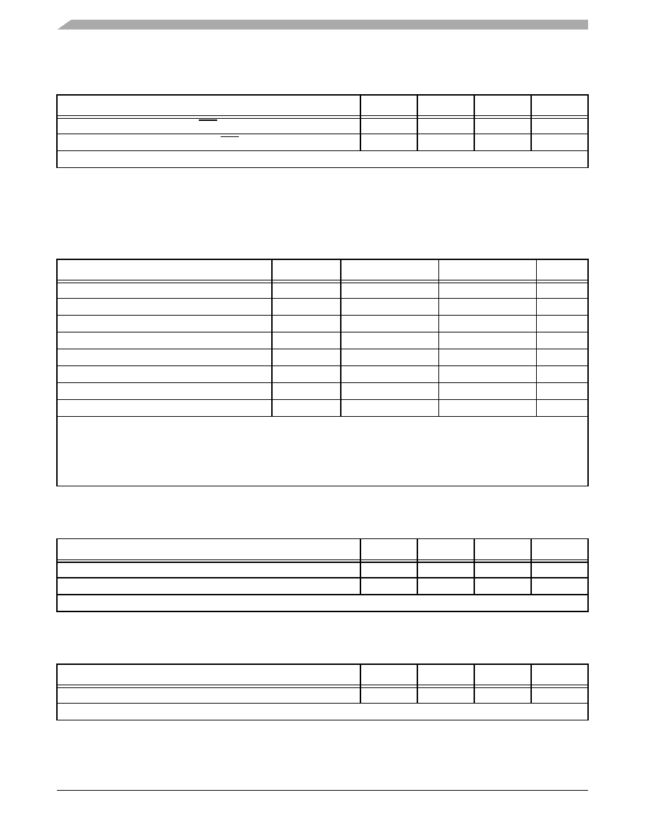
DDR (2.5V) SDRAM DC Electrical Characteristics
Table 10 provides the recommended operating conditions for the DDR SDRAM component(s) of the MSC8144E when
VDDDDR(typ) = 2.5 V.
Table 9. DDR2 SDRAM Capacitance for VDDDDR(typ) = 1.8 V
Parameter/Condition
Symbol
Min
Max
Unit
Input/output capacitance: DQ, DQS, DQS
CIO
68
pF
Delta input/output capacitance: DQ, DQS, DQS
CDIO
—0.5
pF
Note:
This parameter is sampled. VDDDDR = 1.8 V ± 0.090 V, f = 1 MHz, TA =25°C, VOUT = VDDDDR/2, VOUT (peak-to-peak) = 0.2 V.
Table 10. DDR SDRAM DC Electrical Characteristics for VDDDDR (typ) = 2.5 V
Parameter/Condition
Symbol
Min
Max
Unit
I/O supply voltage1
VDDDDR
2.3
2.7
V
I/O reference voltage2
MVREF
0.49
× VDDDDR
0.51
× VDDDDR
V
I/O termination voltage3
VTT
MVREF – 0.04
MVREF + 0.04
V
Input high voltage
VIH
MVREF + 0.15
VDD + 0.3
V
Input low voltage
VIL
–0.3
MVREF – 0.15
V
Output leakage current4
IOZ
–30
30
μA
Output high current (VOUT = 1.95 V)
IOH
–16.2
—
mA
Output low current (VOUT = 0.35 V)
IOL
16.2
—
mA
Notes:
1.
VDDDDR is expected to be within 50 mV of the DRAM VDD at all times.
2.
MVREF is expected to be equal to 0.5 × VDDDDR, and to track VDDDDR DC variations as measured at the receiver.
Peak-to-peak noise on MVREF may not exceed ±2% of the DC value.
3.
VTT is not applied directly to the device. It is the supply to which far end signal termination is made and is expected to be
equal to MVREF. This rail should track variations in the DC level of VDDDDR.
4.
Output leakage is measured with all outputs are disabled, 0 V
≤ V
OUT
≤ V
DDDDR.
Table 11. DDR SDRAM Capacitance for VDDDDR (typ) = 2.5 V
Parameter/Condition
Symbol
Min
Max
Unit
Input/output capacitance: DQ, DQS
CIO
68
pF
Delta input/output capacitance: DQ, DQS
CDIO
—0.5
pF
Note:
This parameter is sampled. VDDDDR = 2.5 V ± 0.125 V, f = 1 MHz, TA = 25°C, VOUT = VDDDDR/2, VOUT (peak-to-peak) = 0.2 V.
Table 12. Current Draw Characteristics for MVREF
Parameter / Condition
Symbol
Min
Max
Unit
Current draw for MVREF
IMVREF
—
500
μA
Note:
The voltage regulator for MVREF must be able to supply up to 500 μA current.
相关PDF资料 |
PDF描述 |
|---|---|
| MSC8152TVT1000B | RISC PROCESSOR, PBGA783 |
| MSC8154ETVT1000B | 0-BIT, OTHER DSP, PBGA783 |
| MSC8252TVT1000B | 0-BIT, OTHER DSP, PBGA783 |
| MSC8252SVT1000B | 0-BIT, OTHER DSP, PBGA783 |
| MSD1010LT3 | 100 mA, 15 V, PNP, Si, SMALL SIGNAL TRANSISTOR |
相关代理商/技术参数 |
参数描述 |
|---|---|
| MSC8144EC | 制造商:FREESCALE 制造商全称:Freescale Semiconductor, Inc 功能描述:Quad Core Digital Signal Processor |
| MSC8144ESVT1000B | 制造商:Freescale Semiconductor 功能描述:DSP 32-BIT 1GHZ 1000MIPS 783-PIN FCBGA BOX - Trays 制造商:Freescale Semiconductor 功能描述:ENCRYPTION PACSUN R2.1 783FCPBGA |
| MSC8144ESVT800A | 制造商:Freescale Semiconductor 功能描述:DSP 32BIT 800MHZ 800MIPS 783FCBGA - Trays |
| MSC8144ESVT800B | 制造商:Freescale Semiconductor 功能描述:DSP 32-BIT 800MHZ 800MIPS 783-PIN FCBGA EACH - Bulk 制造商:Freescale Semiconductor 功能描述:ENCRYPTION PACSUN R2.1 783FCPBGA |
| MSC8144ETVT1000A | 制造商:Freescale Semiconductor 功能描述:DSP 32-BIT 1GHZ 1000MIPS 783-PIN FCBGA - Bulk |
发布紧急采购,3分钟左右您将得到回复。