- 您现在的位置:买卖IC网 > PDF目录186920 > MT2VDDT832UY-75ZXX 8M X 32 DDR DRAM MODULE, 0.75 ns, DMA100 PDF资料下载
参数资料
| 型号: | MT2VDDT832UY-75ZXX |
| 元件分类: | DRAM |
| 英文描述: | 8M X 32 DDR DRAM MODULE, 0.75 ns, DMA100 |
| 封装: | LEAD FREE, DIMM-100 |
| 文件页数: | 9/27页 |
| 文件大小: | 420K |
| 代理商: | MT2VDDT832UY-75ZXX |
第1页第2页第3页第4页第5页第6页第7页第8页当前第9页第10页第11页第12页第13页第14页第15页第16页第17页第18页第19页第20页第21页第22页第23页第24页第25页第26页第27页
32MB, 64MB (x32, SR)
100-PIN DDR UDIMM
pdf: 09005aef808ebdbc, source: 09005aef808e914b
Micron Technology, Inc., reserves the right to change products or specifications without notice.
DD2C8_16x32UG.fm - Rev. D 9/04 EN
17
2004 Micron Technology, Inc. All rights reserved.
Notes
1. All voltages referenced to VSS.
2. Tests for AC timing, IDD, and electrical AC and DC
characteristics may be conducted at nominal ref-
erence/supply voltage levels, but the related spec-
ifications and device operation are guaranteed for
the full voltage range specified.
3. Outputs measured with equivalent load:
4. AC timing and IDD tests may use a VIL-to-VIH
swing of up to 1.5V in the test environment, but
input timing is still referenced to VREF (or to the
crossing point for CK/CK#), and parameter speci-
fications are guaranteed for the specified AC input
levels under normal use conditions. The mini-
mum slew rate for the input signals used to test
the device is 1V/ns in the range between VIL (AC)
and VIH (AC).
5. The AC and DC input level specifications are as
defined in the SSTL_2 Standard (i.e., the receiver
will effectively switch as a result of the signal
crossing the AC input level, and will remain in that
state as long as the signal does not ring back
above [below] the DC input LOW [HIGH] level).
6. VREF is expected to equal VDDQ/2 of the transmit-
ting device and to track variations in the DC level
of the same. Peak-to-peak noise (non-common
mode) on VREF may not exceed ±2 percent of the
DC value. Thus, from VDDQ/2, VREF is allowed
±25mV for DC error and an additional ±25mV for
AC noise. This measurement is to be taken at the
nearest VREF bypass capacitor.
7. VTT is not applied directly to the device. VTT is a
system supply for signal termination resistors, is
expected to be set equal to VREF and must track
variations in the DC level of VREF.
8. IDD is dependent on output loading and cycle
rates. Specified values are obtained with mini-
mum cycle time at CL = 2 for -75Z and CL = 2.5 for
-6 and -75 with the outputs open.
9. Enables on-chip refresh and address counters.
10. IDD specifications are tested after the device is
properly initialized, and is averaged at the defined
cycle rate.
11. This parameter is sampled. VDD = +2.5V ±0.2V,
VDDQ = +2.5V ±0.2V, VREF = VSS, f = 100 MHz,
TA = 25°C, VOUT (DC) = VDDQ/2, VOUT (peak to
peak) = 0.2V. DM input is grouped with I/O pins,
reflecting the fact that they are matched in loading.
12. For slew rates less than 1 V/ns and greater than or
equal to 0.5 V/ns. If slew rate is less than 0.5 V/ns,
timing must be derated: tIS has an additional 50ps
per each 100mV/ns reduction in slew rate from
500 mV/ns, while tIH is unaffected. If slew rate
exceeds 4.5 V/ns, functionality is uncertain. For -
6, slew rates must be
≥ 0.5 V/ns.
13. The CK/CK# input reference level (for timing ref-
erenced to CK/CK#) is the point at which CK and
CK# cross; the input reference level for signals
other than CK/CK# is VREF.
14. Inputs are not recognized as valid until VREF stabi-
lizes. Exception: during the period before VREF
stabilizes, CKE
≤ 0.3 x VDDQ is recognized as LOW.
15. The output timing reference level, as measured at
the timing reference point indicated in Note 3, is
VTT.
16. tHZ and tLZ transitions occur in the same access
time windows as valid data transitions. These
parameters are not referenced to a specific voltage
level, but specify when the device output is no
longer driving (HZ) or begins driving (LZ).
17. The intent of the Don’t Care state after completion
of the postamble is the DQS-driven signal should
either be high, low, or high-Z and that any signal
transition within the input switching region must
follow valid input requirements. That is, if DQS
transitions high [above VIH DC (MIN)] then it must
not transition low (below VIHDC) prior to tDQSH
(MIN).
18. This is not a device limit. The device will operate
with a negative value, but system performance
could be degraded due to bus turnaround.
19. It is recommended that DQS be valid (HIGH or
LOW) on or before the WRITE command. The
case shown (DQS going from High-Z to logic
LOW) applies when no WRITEs were previously in
progress on the bus. If a previous WRITE was in
progress, DQS could be HIGH during this time,
depending on tDQSS.
20. MIN (tRC or tRFC) for IDD measurements is the
smallest multiple of tCK that meets the minimum
absolute value for the respective parameter. tRAS
(MAX) for IDD measurements is the largest multi-
ple of tCK that meets the maximum absolute
value for tRAS.
21. The refresh period 64ms. This equates to an aver-
age refresh rate of 15.625s (32MB) or 7.8125s
(64MB). However, an AUTO REFRESH command
must be asserted at least once every 140.6s
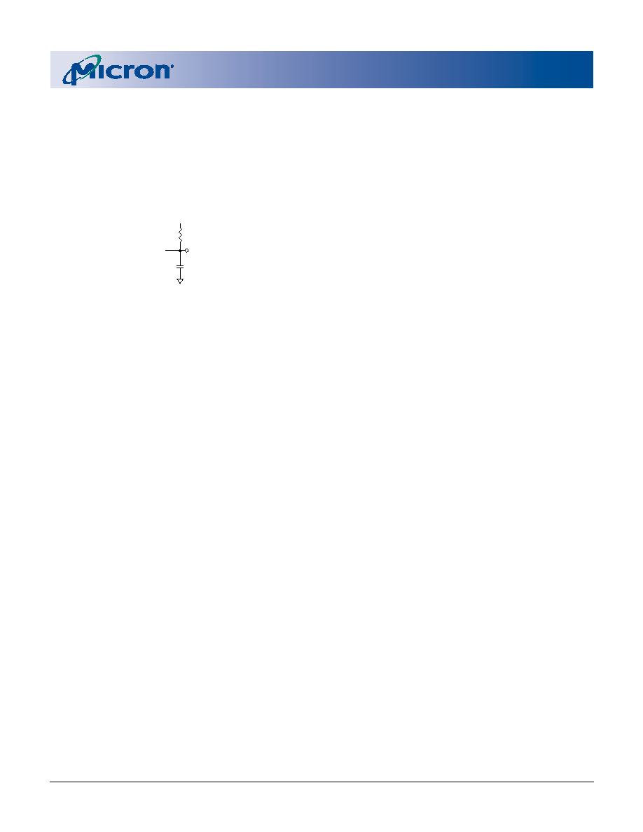
Output
(VOUT)
Reference
Point
50
VTT
30pF
相关PDF资料 |
PDF描述 |
|---|---|
| MT30G1415P9 | 15 CONTACT(S), STAINLESS STEEL, MALE, MIL SERIES CONNECTOR, RECEPTACLE |
| M83723/82K0898N | 3 CONTACT(S), STAINLESS STEEL, MALE OR FEMALE, MIL SERIES CONNECTOR, RECEPTACLE |
| M83723/92S08982 | 3 CONTACT(S), STAINLESS STEEL, MALE OR FEMALE, MIL SERIES CONNECTOR, PLUG |
| M83723/82N0803Y | 3 CONTACT(S), STAINLESS STEEL, MALE OR FEMALE, MIL SERIES CONNECTOR, RECEPTACLE |
| M83723/82S08036 | 3 CONTACT(S), STAINLESS STEEL, MALE OR FEMALE, MIL SERIES CONNECTOR, RECEPTACLE |
相关代理商/技术参数 |
参数描述 |
|---|---|
| MT2-X-00-526-3-A21-B-C | 制造商:Carling Technologies 功能描述:M-SERIES CIRCUIT BREAKER - Bulk |
| MT3 | 功能描述:接线端子工具和配件 Markg Tag 5x10mm Horizontal RoHS:否 制造商:Phoenix Contact 产品:Tools & Accessories 类型:End Bracket |
| MT-3 | 功能描述:烙铁 Weller Chisel Tip For SP23/SP23D RoHS:否 制造商:Weller 产品:Soldering Stations 类型:Digital, Iron, Stand, Cleaner 瓦特:50 W 最大温度:+ 850 F 电缆类型:US Cord Included |
| MT3/H-1 | 功能描述:接线端子工具和配件 Marking Tag, HorizontalImprint "1" RoHS:否 制造商:Phoenix Contact 产品:Tools & Accessories 类型:End Bracket |
| MT3/H-2 | 功能描述:接线端子工具和配件 Marking Tag, HorizontalImprint "2" RoHS:否 制造商:Phoenix Contact 产品:Tools & Accessories 类型:End Bracket |
发布紧急采购,3分钟左右您将得到回复。