- 您现在的位置:买卖IC网 > PDF目录385639 > MT48LC16M4A2 (Micron Technology, Inc.) RSD Series - Econoline Unregulated DC-DC Converters; Input Voltage (Vdc): 24V; Output Voltage (Vdc): 3.3V; Power: 1W; 1kVDC and 3kVDC Isolation Options; Approved for Medical Applications; Suitable for Automated Assembly; 8, 10 and 12 pin Pinning Style Options; Optional Continuous Short Circuit Protected; Efficiency to 85% PDF资料下载
参数资料
| 型号: | MT48LC16M4A2 |
| 厂商: | Micron Technology, Inc. |
| 元件分类: | DC/DC变换器 |
| 英文描述: | RSD Series - Econoline Unregulated DC-DC Converters; Input Voltage (Vdc): 24V; Output Voltage (Vdc): 3.3V; Power: 1W; 1kVDC and 3kVDC Isolation Options; Approved for Medical Applications; Suitable for Automated Assembly; 8, 10 and 12 pin Pinning Style Options; Optional Continuous Short Circuit Protected; Efficiency to 85% |
| 中文描述: | 同步DRAM |
| 文件页数: | 1/55页 |
| 文件大小: | 1458K |
| 代理商: | MT48LC16M4A2 |
当前第1页第2页第3页第4页第5页第6页第7页第8页第9页第10页第11页第12页第13页第14页第15页第16页第17页第18页第19页第20页第21页第22页第23页第24页第25页第26页第27页第28页第29页第30页第31页第32页第33页第34页第35页第36页第37页第38页第39页第40页第41页第42页第43页第44页第45页第46页第47页第48页第49页第50页第51页第52页第53页第54页第55页
1
64Mb: x4, x8, x16 SDRAM
64MSDRAM_F.p65 – Rev. F; Pub. 1/03
Micron Technology, Inc., reserves the right to change products or specifications without notice.
2003, Micron Technology, Inc.
64Mb: x4, x8, x16
SDRAM
16 Meg x 4
4 Meg x 4 x 4 banks
4K
4K (A0-A11)
4 (BA0, BA1)
1K (A0-A9)
8 Meg x 8
2 Meg x 8 x 4 banks
4K
4K (A0-A11)
4 (BA0, BA1)
512 (A0-A8)
4 Meg x 16
1 Meg x 16 x 4 banks
4K
4K (A0-A11)
4 (BA0, BA1)
256 (A0-A7)
Configuration
Refresh Count
Row Addressing
Bank Addressing
Column Addressing
SYNCHRONOUS
DRAM
MT48LC16M4A2 – 4 Meg x 4
MT48LC8M8A2 –
MT48LC4M16A2 – 1 Meg x 16 x 4 banks
For the latest data sheet, please refer to the Micron Web
site:
www.micron.com/dramds
x 4 banks
x 4 banks
2 Meg x 8
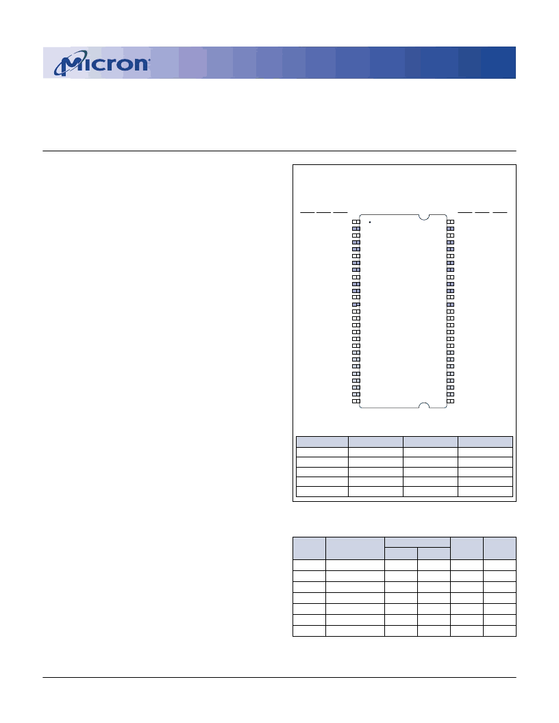
PIN ASSIGNMENT (Top View )
54-Pin TSOP
FEATURES
PC66-, PC100-, and PC133-compliant
Fully synchronous; all signals registered on
positive edge of system clock
Internal pipelined operation; column address can
be changed every clock cycle
Internal banks for hiding row access/precharge
Programmable burst lengths: 1, 2, 4, 8, or full page
Auto Precharge, includes CONCURRENT AUTO
PRECHARGE, and Auto Refresh Modes
Self Refresh Modes: standard and low power
64ms, 4,096-cycle refresh
LVTTL-compatible inputs and outputs
Single +3.3V ±0.3V power supply
OPTIONS
Configurations
16 Meg x 4
8 Meg x 8
4 Meg x 16 (1 Meg x 16 x 4 banks)
MARKING
(4 Meg x 4
(2 Meg x 8
x 4 banks)
x 4 banks)
16M4
8M8
4M16
WRITE Recovery (
t
WR)
t
WR = “2 CLK”
1
A2
Plastic Package – OCPL
2
54-pin TSOP II (400 mil)
TG
Timing (Cycle Time)
10ns @ CL = 2 (PC100)
7.5ns @ CL = 3 (PC133)
7.5ns @ CL = 2 (PC133)
6ns @ CL = 3 (PC133, x16 Only)
-8E
3, 4,5
-75
-7E
-6
Self Refresh
Standard
Low Power
None
L
Operating Temperature Range
Commercial (0°C to +70°C)
Industrial (-40°C to +85°C)
None
IT
3
Part Number Example:
MT48LC8M8A2TG-75
NOTE
: 1. Refer to Micron Technical Note: TN-48-05.
2. Off-center parting line.
3. Consult Micron for availability.
4. Not recommended for new designs.
5. Shown for PC100 compatibility.
V
DD
DQ0
V
DD
Q
DQ1
DQ2
VssQ
DQ3
DQ4
V
DD
Q
DQ5
DQ6
VssQ
DQ7
V
DD
DQML
WE#
CAS#
RAS#
CS#
BA0
BA1
A10
A0
A1
A2
A3
V
DD
1
2
3
4
5
6
7
8
9
10
11
12
13
14
15
16
17
18
19
20
21
22
23
24
25
26
27
54
53
52
51
50
49
48
47
46
45
44
43
42
41
40
39
38
37
36
35
34
33
32
31
30
29
28
Vss
DQ15
VssQ
DQ14
DQ13
V
DD
Q
DQ12
DQ11
VssQ
DQ10
DQ9
V
DD
Q
DQ8
Vss
NC
DQMH
CLK
CKE
NC
A11
A9
A8
A7
A6
A5
A4
Vss
x8
-
DQ7
-
NC
DQ6
-
NC
DQ5
-
NC
DQ4
-
NC
-
-
DQM
-
-
-
-
-
-
-
-
-
-
-
x16
x16
x8
-
DQ0
-
NC
DQ1
-
NC
DQ2
-
NC
DQ3
-
NC
-
NC
-
-
-
-
-
-
-
-
-
-
-
-
x4
-
NC
-
NC
DQ3
-
NC
NC
-
NC
DQ2
-
NC
-
-
DQM
-
-
-
-
-
-
-
-
-
-
-
x4
-
NC
-
NC
DQ0
-
NC
NC
-
NC
DQ1
-
NC
-
NC
-
-
-
-
-
-
-
-
-
-
-
-
Note:
The # symbol indicates signal is active LOW. A dash (–)
indicates x8 and x4 pin function is same as x16 pin function.
KEY TIMING PARAMETERS
SPEED
GRADE
-6
-7E
-75
-7E
-8E
3, 4, 5
-75
-8E
3, 4, 5
CLOCK
FREQUENCY
166 MHz
143 MHz
133 MHz
133 MHz
125 MHz
100 MHz
100 MHz
ACCESS TIME
CL = 2* CL = 3*
–
–
–
5.4ns
–
6ns
6ns
SETUP
TIME
1.5ns
1.5ns
1.5ns
1.5ns
2ns
1.5ns
2ns
HOLD
TIME
1ns
0.8ns
0.8ns
0.8ns
1ns
0.8ns
1ns
5.5ns
5.4ns
5.4ns
–
6ns
–
–
* CL = CAS (READ) latency
相关PDF资料 |
PDF描述 |
|---|---|
| MT48LC8M16A2 | SYNCHRONOUS DRAM |
| MT48V2M32LFFC | 512K x 32 x 4 banks 2.5V SDRAM(2.5V,512K x 32 x 4组同步动态RAM) |
| MT48V4M32LFFC | SYNCHRONOUS DRAM |
| MT49H16M16 | THERMISTOR PTC 100OHM 110DEG RAD |
| MT49H16M16FM | REDUCED LATENCY DRAM RLDRAM |
相关代理商/技术参数 |
参数描述 |
|---|---|
| MT48LC16M4A2_99 | 制造商:MICRON 制造商全称:Micron Technology 功能描述:SYNCHRONOUS DRAM |
| MT48LC16M4A2TG | 制造商:MICRON 制造商全称:Micron Technology 功能描述:SYNCHRONOUS DRAM |
发布紧急采购,3分钟左右您将得到回复。