- 您现在的位置:买卖IC网 > PDF目录385639 > MT48LC16M4A2 (Micron Technology, Inc.) RSD Series - Econoline Unregulated DC-DC Converters; Input Voltage (Vdc): 24V; Output Voltage (Vdc): 3.3V; Power: 1W; 1kVDC and 3kVDC Isolation Options; Approved for Medical Applications; Suitable for Automated Assembly; 8, 10 and 12 pin Pinning Style Options; Optional Continuous Short Circuit Protected; Efficiency to 85% PDF资料下载
参数资料
| 型号: | MT48LC16M4A2 |
| 厂商: | Micron Technology, Inc. |
| 元件分类: | DC/DC变换器 |
| 英文描述: | RSD Series - Econoline Unregulated DC-DC Converters; Input Voltage (Vdc): 24V; Output Voltage (Vdc): 3.3V; Power: 1W; 1kVDC and 3kVDC Isolation Options; Approved for Medical Applications; Suitable for Automated Assembly; 8, 10 and 12 pin Pinning Style Options; Optional Continuous Short Circuit Protected; Efficiency to 85% |
| 中文描述: | 同步DRAM |
| 文件页数: | 9/55页 |
| 文件大小: | 1458K |
| 代理商: | MT48LC16M4A2 |
第1页第2页第3页第4页第5页第6页第7页第8页当前第9页第10页第11页第12页第13页第14页第15页第16页第17页第18页第19页第20页第21页第22页第23页第24页第25页第26页第27页第28页第29页第30页第31页第32页第33页第34页第35页第36页第37页第38页第39页第40页第41页第42页第43页第44页第45页第46页第47页第48页第49页第50页第51页第52页第53页第54页第55页
9
64Mb: x4, x8, x16 SDRAM
64MSDRAM_F.p65 – Rev. F; Pub. 1/03
Micron Technology, Inc., reserves the right to change products or specifications without notice.
2003, Micron Technology, Inc.
64Mb: x4, x8, x16
SDRAM
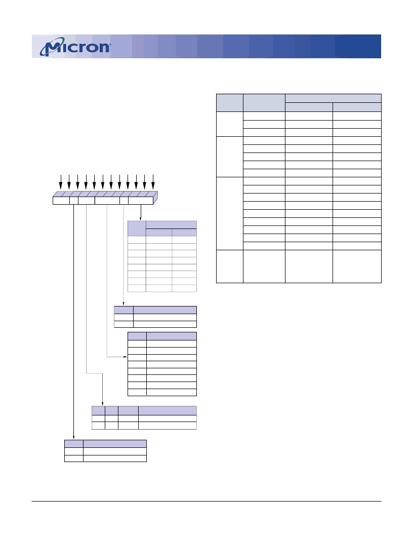
NOTE:
1. For full-page accesses: y = 1,024 (x4); y = 512 (x8);
y = 256 (x16).
2. For a burst length of two, A1-A9 (x4), A1-A8 (x8),
or A1-A7 (x16) select the block-of-two burst; A0
selects the starting column within the block.
3. For a burst length of four, A2-A9 (x4), A2-A8 (x8),
or A2-A7 (x16) select the block-of-four burst; A0-
A1 select the starting column within the block.
4. For a burst length of eight, A3-A9 (x4), A3-A8 (x8),
or A3-A7 (x16) select the block-of-eight burst; A0-
A2 select the starting column within the block.
5. For a full-page burst, the full row is selected and
A0-A9 (x4), A0-A8 (x8), or A0-A7 (x16) select the
starting column.
6. Whenever a boundary of the block is reached
within a given sequence above, the following
access wraps within the block.
7. For a burst length of one, A0-A9 (x4), A0-A8 (x8),
or A0-A7 (x16) select the unique column to be
accessed, and mode register bit M3 is ignored.
Table 1
Burst Definition
Burst
Length
Starting Column
Address
Order of Accesses Within a Burst
Type = Sequential
Type = Interleaved
A0
0
1
2
0-1
1-0
0-1
1-0
A1 A0
0
0
1
1
0
1
0
1
0-1-2-3
1-2-3-0
2-3-0-1
3-0-1-2
0-1-2-3
1-0-3-2
2-3-0-1
3-2-1-0
4
A2 A1 A0
0
0
0
0
0
1
0
1
1
0
1
0
1
1
1
1
0
1
0
1
0
1
0
1
0-1-2-3-4-5-6-7
1-2-3-4-5-6-7-0
2-3-4-5-6-7-0-1
3-4-5-6-7-0-1-2
4-5-6-7-0-1-2-3
5-6-7-0-1-2-3-4
6-7-0-1-2-3-4-5
7-0-1-2-3-4-5-6
Cn, Cn + 1, Cn + 2
Cn + 3, Cn + 4...
…Cn - 1,
Cn…
0-1-2-3-4-5-6-7
1-0-3-2-5-4-7-6
2-3-0-1-6-7-4-5
3-2-1-0-7-6-5-4
4-5-6-7-0-1-2-3
5-4-7-6-1-0-3-2
6-7-4-5-2-3-0-1
7-6-5-4-3-2-1-0
8
Full
Page
(y)
n = A0-A9/8/7
Not Supported
(location 0-y)
M3 = 0
1
2
4
8
Reserved
Reserved
Reserved
Full Page
M3 = 1
1
2
4
8
Reserved
Reserved
Reserved
Reserved
Operating Mode
Standard Operation
All other states reserved
0
-
0
-
Defined
-
0
1
Burst Type
Sequential
Interleaved
CAS Latency
Reserved
Reserved
2
3
Reserved
Reserved
Reserved
Reserved
Burst Length
M0
0
1
0
1
0
1
0
1
Burst Length
CAS Latency
BT
A9
A7
A6
A5
A4
A3
A8
A2
A1
A0
Mode Register (Mx)
Address Bus
9
7
6
5
4
3
8
2
1
0
M1
0
0
1
1
0
0
1
1
M2
0
0
0
0
1
1
1
1
M3
M4
0
1
0
1
0
1
0
1
M5
0
0
1
1
0
0
1
1
M6
0
0
0
0
1
1
1
1
M6-M0
M8
M7
Op Mode
A10
A11
10
11
Reserved* WB
0
1
Write Burst Mode
Programmed Burst Length
Single Location Access
M9
*Should program
M11, M10 = “0, 0”
to ensure compatibility
with future devices.
Figure 1
Mode Register Definition
Burst Type
Accesses within a given burst may be programmed
to be either sequential or interleaved; this is referred to
as the burst type and is selected via bit M3.
The ordering of accesses within a burst is deter-
mined by the burst length, the burst type and the start-
ing column address, as shown in Table 1.
相关PDF资料 |
PDF描述 |
|---|---|
| MT48LC8M16A2 | SYNCHRONOUS DRAM |
| MT48V2M32LFFC | 512K x 32 x 4 banks 2.5V SDRAM(2.5V,512K x 32 x 4组同步动态RAM) |
| MT48V4M32LFFC | SYNCHRONOUS DRAM |
| MT49H16M16 | THERMISTOR PTC 100OHM 110DEG RAD |
| MT49H16M16FM | REDUCED LATENCY DRAM RLDRAM |
相关代理商/技术参数 |
参数描述 |
|---|---|
| MT48LC16M4A2_99 | 制造商:MICRON 制造商全称:Micron Technology 功能描述:SYNCHRONOUS DRAM |
| MT48LC16M4A2TG | 制造商:MICRON 制造商全称:Micron Technology 功能描述:SYNCHRONOUS DRAM |
发布紧急采购,3分钟左右您将得到回复。