- 您现在的位置:买卖IC网 > PDF目录385639 > MT48LC16M4A2 (Micron Technology, Inc.) RSD Series - Econoline Unregulated DC-DC Converters; Input Voltage (Vdc): 24V; Output Voltage (Vdc): 3.3V; Power: 1W; 1kVDC and 3kVDC Isolation Options; Approved for Medical Applications; Suitable for Automated Assembly; 8, 10 and 12 pin Pinning Style Options; Optional Continuous Short Circuit Protected; Efficiency to 85% PDF资料下载
参数资料
| 型号: | MT48LC16M4A2 |
| 厂商: | Micron Technology, Inc. |
| 元件分类: | DC/DC变换器 |
| 英文描述: | RSD Series - Econoline Unregulated DC-DC Converters; Input Voltage (Vdc): 24V; Output Voltage (Vdc): 3.3V; Power: 1W; 1kVDC and 3kVDC Isolation Options; Approved for Medical Applications; Suitable for Automated Assembly; 8, 10 and 12 pin Pinning Style Options; Optional Continuous Short Circuit Protected; Efficiency to 85% |
| 中文描述: | 同步DRAM |
| 文件页数: | 24/55页 |
| 文件大小: | 1458K |
| 代理商: | MT48LC16M4A2 |
第1页第2页第3页第4页第5页第6页第7页第8页第9页第10页第11页第12页第13页第14页第15页第16页第17页第18页第19页第20页第21页第22页第23页当前第24页第25页第26页第27页第28页第29页第30页第31页第32页第33页第34页第35页第36页第37页第38页第39页第40页第41页第42页第43页第44页第45页第46页第47页第48页第49页第50页第51页第52页第53页第54页第55页
24
64Mb: x4, x8, x16 SDRAM
64MSDRAM_F.p65 – Rev. F; Pub. 1/03
Micron Technology, Inc., reserves the right to change products or specifications without notice.
2003, Micron Technology, Inc.
64Mb: x4, x8, x16
SDRAM
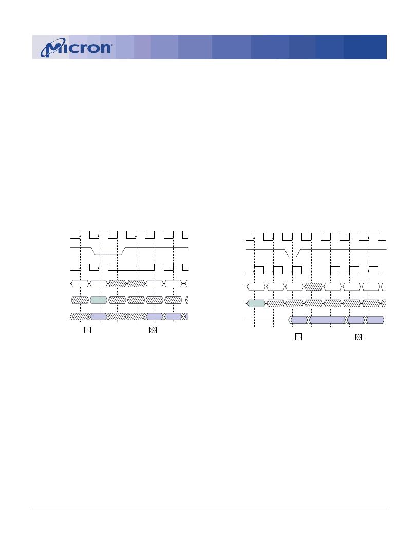
Figure 22
Clock Suspend During WRITE Burst
Figure 23
Clock Suspend During READ Burst
CLOCK SUSPEND
The clock suspend mode occurs when a column ac-
cess/burst is in progress and CKE is registered LOW. In
the clock suspend mode, the internal clock is deacti-
vated, “freezing” the synchronous logic.
For each positive clock edge on which CKE is
sampled LOW, the next internal positive clock edge is
suspended. Any command or data present on the in-
put pins at the time of a suspended internal clock edge
is ignored; any data present on the DQ pins remains
driven; and burst counters are not incremented, as
long as the clock is suspended. (See examples in
Figures 22 and 23.)
Clock suspend mode is exited by registering CKE
HIGH; the internal clock and related operation will re-
sume on the subsequent positive clock edge.
BURST READ/SINGLE WRITE
The burst read/single write mode is entered by pro-
gramming the write burst mode bit (M9) in the mode
register to a logic 1. In this mode, all WRITE commands
result in the access of a single column location (burst of
one), regardless of the programmed burst length. READ
commands access columns according to the pro-
grammed burst length and sequence, just as in the
normal mode of operation (M9 = 0).
DON’T CARE
D
IN
COMMAND
ADDRESS
WRITE
BANK,
COL
n
D
IN
n
NOP
NOP
CLK
T2
T1
T4
T3
T5
T0
CKE
INTERNAL
CLOCK
NOP
D
IN
n
+ 1
D
IN
n
+ 2
TRANSITIONING DATA
DON’T CARE
CLK
DQ
D
OUT
n
T2
T1
T4
T3
T6
T5
T0
COMMAND
ADDRESS
READ
NOP
NOP
NOP
BANK,
COL
n
NOP
D
OUT
n
+ 1
D
OUT
n
+ 2
D
OUT
n
+ 3
NOTE:
For this example, CAS latency = 2, burst length = 4 or greater, and
DQM is LOW.
CKE
INTERNAL
CLOCK
NOP
TRANSITIONING DATA
相关PDF资料 |
PDF描述 |
|---|---|
| MT48LC8M16A2 | SYNCHRONOUS DRAM |
| MT48V2M32LFFC | 512K x 32 x 4 banks 2.5V SDRAM(2.5V,512K x 32 x 4组同步动态RAM) |
| MT48V4M32LFFC | SYNCHRONOUS DRAM |
| MT49H16M16 | THERMISTOR PTC 100OHM 110DEG RAD |
| MT49H16M16FM | REDUCED LATENCY DRAM RLDRAM |
相关代理商/技术参数 |
参数描述 |
|---|---|
| MT48LC16M4A2_99 | 制造商:MICRON 制造商全称:Micron Technology 功能描述:SYNCHRONOUS DRAM |
| MT48LC16M4A2TG | 制造商:MICRON 制造商全称:Micron Technology 功能描述:SYNCHRONOUS DRAM |
发布紧急采购,3分钟左右您将得到回复。