- 您现在的位置:买卖IC网 > PDF目录385639 > MT48LC16M4A2 (Micron Technology, Inc.) RSD Series - Econoline Unregulated DC-DC Converters; Input Voltage (Vdc): 24V; Output Voltage (Vdc): 3.3V; Power: 1W; 1kVDC and 3kVDC Isolation Options; Approved for Medical Applications; Suitable for Automated Assembly; 8, 10 and 12 pin Pinning Style Options; Optional Continuous Short Circuit Protected; Efficiency to 85% PDF资料下载
参数资料
| 型号: | MT48LC16M4A2 |
| 厂商: | Micron Technology, Inc. |
| 元件分类: | DC/DC变换器 |
| 英文描述: | RSD Series - Econoline Unregulated DC-DC Converters; Input Voltage (Vdc): 24V; Output Voltage (Vdc): 3.3V; Power: 1W; 1kVDC and 3kVDC Isolation Options; Approved for Medical Applications; Suitable for Automated Assembly; 8, 10 and 12 pin Pinning Style Options; Optional Continuous Short Circuit Protected; Efficiency to 85% |
| 中文描述: | 同步DRAM |
| 文件页数: | 7/55页 |
| 文件大小: | 1458K |
| 代理商: | MT48LC16M4A2 |
第1页第2页第3页第4页第5页第6页当前第7页第8页第9页第10页第11页第12页第13页第14页第15页第16页第17页第18页第19页第20页第21页第22页第23页第24页第25页第26页第27页第28页第29页第30页第31页第32页第33页第34页第35页第36页第37页第38页第39页第40页第41页第42页第43页第44页第45页第46页第47页第48页第49页第50页第51页第52页第53页第54页第55页
7
64Mb: x4, x8, x16 SDRAM
64MSDRAM_F.p65 – Rev. F; Pub. 1/03
Micron Technology, Inc., reserves the right to change products or specifications without notice.
2003, Micron Technology, Inc.
64Mb: x4, x8, x16
SDRAM
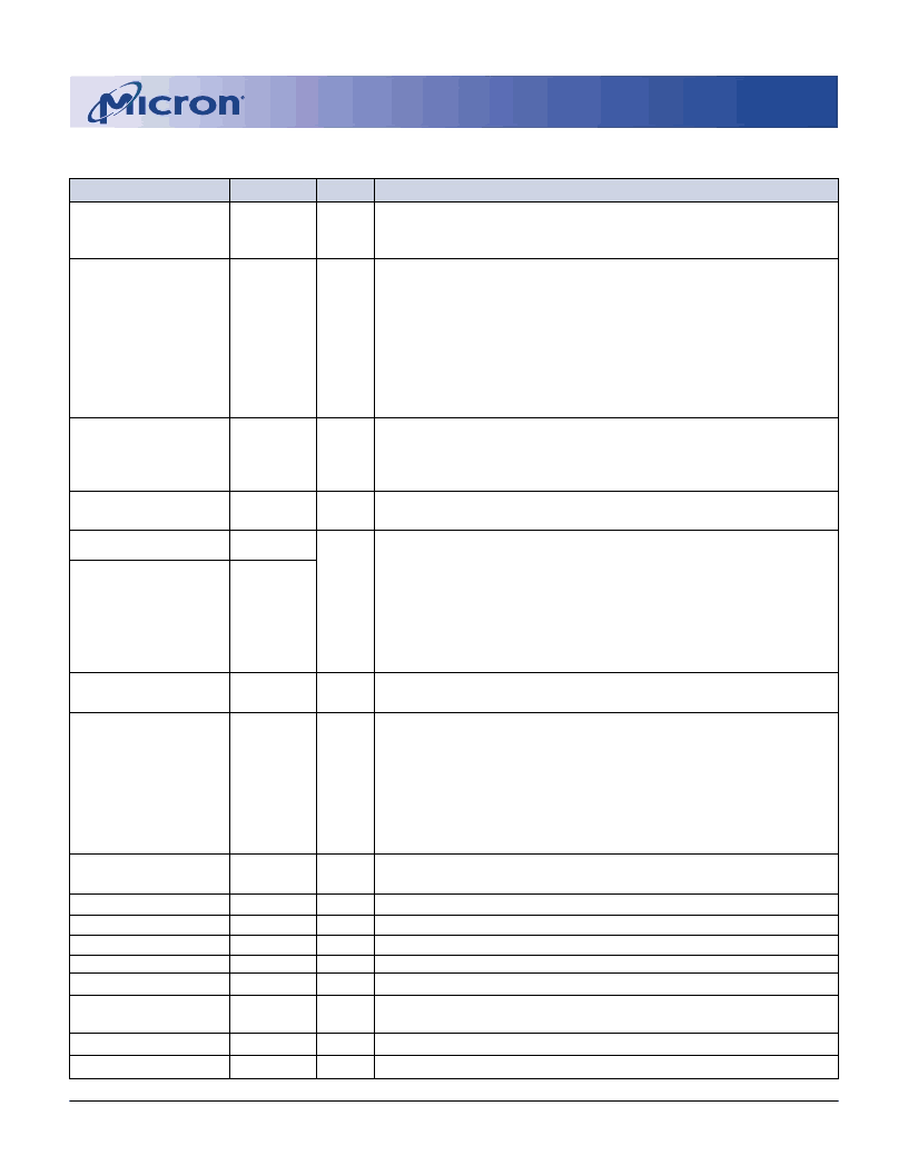
PIN DESCRIPTIONS
PIN NUMBERS
38
SYMBOL
CLK
TYPE
Input
DESCRIPTION
Clock: CLK is driven by the system clock. All SDRAM input signals are
sampled on the positive edge of CLK. CLK also increments the internal
burst counter and controls the output registers.
Clock Enable: CKE activates (HIGH) and deactivates (LOW) the CLK
signal. Deactivating the clock provides PRECHARGE POWER-DOWN
and SELF REFRESH operation (all banks idle), ACTIVE POWER-DOWN
(row active in any bank) or CLOCK SUSPEND operation (burst/access in
progress). CKE is synchronous except after the device enters power-
down and self refresh modes, where CKE becomes asynchronous until
after exiting the same mode. The input buffers, including CLK, are
disabled during power-down and self refresh modes, providing low
standby power. CKE may be tied HIGH.
Chip Select: CS# enables (registered LOW) and disables (registered
HIGH) the command decoder. All commands are masked when CS# is
registered HIGH. CS# provides for external bank selection on systems
with multiple banks. CS# is considered part of the command code.
Command Inputs: WE#, CAS#, and RAS# (along with CS#) define the
command being entered.
Input/Output Mask: DQM is an input mask signal for write accesses and
an output enable signal for read accesses. Input data is masked when
DQM is sampled HIGH during a WRITE cycle. The output buffers are
placed in a High-Z state (two-clock latency) when DQM is sampled
HIGH during a READ cycle. On the x4 and x8, DQML (Pin 15) is a NC
and DQMH is DQM. On the x16, DQML corresponds to DQ0-DQ7 and
DQMH corresponds to DQ8-DQ15. DQML and DQMH are considered
same state when referenced as DQM.
Bank Address Inputs: BA0 and BA1 define to which bank the ACTIVE,
READ, WRITE or PRECHARGE command is being applied.
Address Inputs: A0-A11 are sampled during the ACTIVE command
(row-address A0-A11) and READ/WRITE command (column-address A0-
A9 [x4]; A0-A8 [x8]; A0-A7 [x16]; with A10 defining auto precharge) to
select one location out of the memory array in the respective bank.
A10 is sampled during a PRECHARGE command to determine if all
banks are to be precharged (A10[HIGH]) or bank selected by BA0,
BA1 (A1[LOW]). The address inputs also provide the op-code
during a LOAD MODE REGISTER command.
37
CKE
Input
19
CS#
Input
16, 17, 18
WE#, CAS#,
RAS#
x4, x8: DQM
Input
39
Input
15, 39
x16: DQML,
DQMH
20, 21
BA0, BA1
Input
23-26, 29-34, 22, 35
A0-A11
Input
2, 4, 5, 7, 8, 10, 11, 13, 42, DQ0-DQ15
x16: I/O Data Input/Output: Data bus for x16 (4, 7, 10, 13, 42, 45, 48, and 51 are
44, 45, 47, 48, 50, 51, 53
NCs for x8; and 2, 4, 7, 8, 10, 13, 42, 45, 47, 48, 51, and 53 are NCs for x4).
2, 5, 8, 11, 44, 47, 50, 53
DQ0-DQ7
x8: I/O
Data Input/Output: Data bus for x8 (2, 8, 47, 53 are NCs for x4).
5, 11, 44, 50
DQ0-DQ3
x4: I/O
Data Input/Output: Data bus for x4.
40
NC
–
No Connect: These pins should be left unconnected.
36
NC
–
Address input (A12) for the 256Mb and 512Mb devices
3, 9, 43, 49
V
DD
Q
Supply DQ Power: Isolated DQ power on the die for improved noise immunity.
6, 12, 46, 52
V
SS
Q
Supply DQ Ground: Isolated DQ ground on the die for improved noise
immunity.
1, 14, 27
V
DD
Supply Power Supply: +3.3V ±0.3V.
28, 41, 54
V
SS
Supply Ground.
相关PDF资料 |
PDF描述 |
|---|---|
| MT48LC8M16A2 | SYNCHRONOUS DRAM |
| MT48V2M32LFFC | 512K x 32 x 4 banks 2.5V SDRAM(2.5V,512K x 32 x 4组同步动态RAM) |
| MT48V4M32LFFC | SYNCHRONOUS DRAM |
| MT49H16M16 | THERMISTOR PTC 100OHM 110DEG RAD |
| MT49H16M16FM | REDUCED LATENCY DRAM RLDRAM |
相关代理商/技术参数 |
参数描述 |
|---|---|
| MT48LC16M4A2_99 | 制造商:MICRON 制造商全称:Micron Technology 功能描述:SYNCHRONOUS DRAM |
| MT48LC16M4A2TG | 制造商:MICRON 制造商全称:Micron Technology 功能描述:SYNCHRONOUS DRAM |
发布紧急采购,3分钟左右您将得到回复。