- 您现在的位置:买卖IC网 > PDF目录385639 > MT4C1M16E5DJ-6 (Micron Technology, Inc.) EDO DRAM PDF资料下载
参数资料
| 型号: | MT4C1M16E5DJ-6 |
| 厂商: | Micron Technology, Inc. |
| 英文描述: | EDO DRAM |
| 中文描述: | EDO公司的DRAM |
| 文件页数: | 2/24页 |
| 文件大小: | 385K |
| 代理商: | MT4C1M16E5DJ-6 |
2
1 Meg x 16 EDO DRAM
D52_B.p65 – Rev. B; Pub. 3/01
Micron Technology, Inc., reserves the right to change products or specifications without notice.
2001, Micron Technology, Inc
16Mb: 1 MEG x16
EDO DRAM
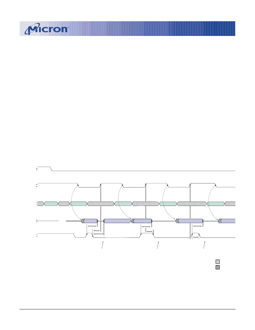
Figure 1
OE# Control of DQs
V
IL
CASL#/CASH#
V
IL
RAS#
V
IL
ADDR
ROW
COLUMN (A)
COLUMN (B)
DON’T CARE
UNDEFINED
V
IL
OE#
V
IOL
OPEN
DQ
tOD
VALID DATA (B)
VALID DATA (A)
COLUMN (C)
VALID DATA (A)
tOE
VALID DATA (C)
COLUMN (D)
VALID DATA (D)
tOD
tOEHC
tOD
tOEP
tOES
The DQs go back to
Low-Z if
OES is met.
The DQs remain High-Z
until the next CAS# cycle
if
OEHC is met.
The DQs remain High-Z
until the next CAS# cycle
if
OEP is met.
A logic HIGH on WE# dictates read mode, while a
logic LOW on WE# dictates write mode. During a WRITE
cycle, data-in (D) is latched by the falling edge of WE or
CAS# (CASL# or CASH#), whichever occurs last. An
EARLY WRITE occurs when WE is taken LOW prior to
either CAS# falling. A LATE WRITE or READ-MODIFY-
WRITE occurs when WE falls after CAS# (CASL# or
CASH#) was taken LOW. During EARLY WRITE cycles,
the data outputs (Q) will remain High-Z, regardless of
the state of OE#. During LATE WRITE or READ-
MODIFY-WRITE cycles, OE# must be taken HIGH to
disable the data outputs prior to applying input data.
If a LATE WRITE or READ-MODIFY-WRITE is attempted
while keeping OE# LOW, no WRITE will occur, and the
data outputs will drive read data from the accessed
location.
The 16 data inputs and 16 data outputs are routed
through 16 pins using common I/O. Pin direction is
controlled by OE# and WE#.
The 1 Meg x 16 DRAM must be refreshed periodi-
cally in order to retain stored data.
of the two signals results in a BYTE WRITE cycle. CASL#
transitioning LOW selects an access cycle for the lower
byte (DQ0-DQ7), and CASH# transitioning LOW se-
lects an access cycle for the upper byte (DQ8-DQ15).
Each bit is uniquely addressed through the 20 ad-
dress bits during READ or WRITE cycles. These are
entered 10 bits (A0-A9) at a time. RAS# is used to latch
the first 10 bits and CAS#, the latter 10 bits.
The CAS#
function also determines whether the cycle will be a
refresh cycle (RAS# ONLY) or an active cycle (READ,
WRITE or READ-WRITE) once RAS# goes LOW.
The CASL# and CASH# inputs internally generate a
CAS# signal that functions like the single CAS# input
on other DRAMs. The key difference is each CAS# input
(CASL# and CASH#) controls its corresponding eight
DQ inputs during WRITE accesses. CASL# controls
DQ0-DQ7, and CASH# controls DQ8-DQ15. The two
CAS# controls give the 1 Meg x 16 both BYTE READ and
BYTE WRITE cycle capabilities.
GENERAL DESCRIPTION (continued)
相关PDF资料 |
PDF描述 |
|---|---|
| MT4LC1M16E5DJ-6S | EDO DRAM |
| MT4LC1M16E5 | EDO DRAM |
| MT4C4256 | 256K x 4 DRAM Standard Or Low Power, Extended Refresh(标准或低功率,扩展刷新,256K x 4动态RAM) |
| MT4C4256L | 256K x 4 DRAM Standard Or Low Power, Extended Refresh(标准或低功率,扩展刷新,256K x 4动态RAM) |
| MT4LC16M4T8TG-5 | DRAM |
相关代理商/技术参数 |
参数描述 |
|---|---|
| MT4C1M16E5TG-5 | 制造商:MICRON 制造商全称:Micron Technology 功能描述:EDO DRAM |
| MT4C1M16E5TG-6 | 制造商:MICRON 制造商全称:Micron Technology 功能描述:EDO DRAM |
| MT4C2M8B1DJ-6 | 制造商:Micron Technology Inc 功能描述: |
| MT4C2M8E7DW-6 | 制造商:Micron Technology Inc 功能描述:2M X 8 EDO DRAM, 60 ns, PDSO28 |
| MT4C40004 | 制造商:MICRON 制造商全称:Micron Technology 功能描述:4 MEG x 4 DRAM |
发布紧急采购,3分钟左右您将得到回复。