- 您现在的位置:买卖IC网 > PDF目录98046 > MTD3302 (ON SEMICONDUCTOR) 8300 mA, 30 V, N-CHANNEL, Si, SMALL SIGNAL, MOSFET PDF资料下载
参数资料
| 型号: | MTD3302 |
| 厂商: | ON SEMICONDUCTOR |
| 元件分类: | 小信号晶体管 |
| 英文描述: | 8300 mA, 30 V, N-CHANNEL, Si, SMALL SIGNAL, MOSFET |
| 封装: | DPAK-3 |
| 文件页数: | 12/12页 |
| 文件大小: | 278K |
| 代理商: | MTD3302 |
MTD3302
http://onsemi.com
9
INFORMATION FOR USING THE DPAK SURFACE MOUNT PACKAGE
RECOMMENDED FOOTPRINT FOR SURFACE MOUNTED APPLICATIONS
Surface mount board layout is a critical portion of the
total design. The footprint for the semiconductor packages
must be the correct size to ensure proper solder connection
interface between the board and the package. With the
correct pad geometry, the packages will self align when
subjected to a solder reflow process.
0.190
4.826
mm
inches
0.100
2.54
0.063
1.6
0.165
4.191
0.118
3.0
0.243
6.172
POWER DISSIPATION FOR A SURFACE MOUNT DEVICE
The power dissipation for a surface mount device is a
function of the drain pad size. These can vary from the
minimum pad size for soldering to a pad size given for
maximum power dissipation. Power dissipation for a
surface mount device is determined by TJ(max), the
maximum rated junction temperature of the die, RθJA, the
thermal resistance from the device junction to ambient, and
the operating temperature, TA. Using the values provided
on the data sheet, PD can be calculated as follows:
PD =
TJ(max) TA
RθJA
The values for the equation are found in the maximum
ratings table on the data sheet. Substituting these values
into the equation for an ambient temperature TA of 25°C,
one can calculate the power dissipation of the device. For a
DPAK device, PD is calculated as follows.
PD =
150
°C 25°C
71.4
°C/W
= 1.75 Watts
The 71.4
°C/W for the DPAK package assumes the use of
the recommended footprint on a glass epoxy printed circuit
board to achieve a power dissipation of 1.75 Watts. Note
that these values may vary depending on the device type.
Consult the maximum ratings table on the data sheet to find
the actual PD and RqJA values for a particular device. There
are other alternatives to achieving higher power dissipation
from the surface mount packages. One is to increase the
area of the drain pad. By increasing the area of the drain
pad, the power dissipation can be increased. Although one
can almost double the power dissipation with this method,
one will be giving up area on the printed circuit board
which can defeat the purpose of using surface mount
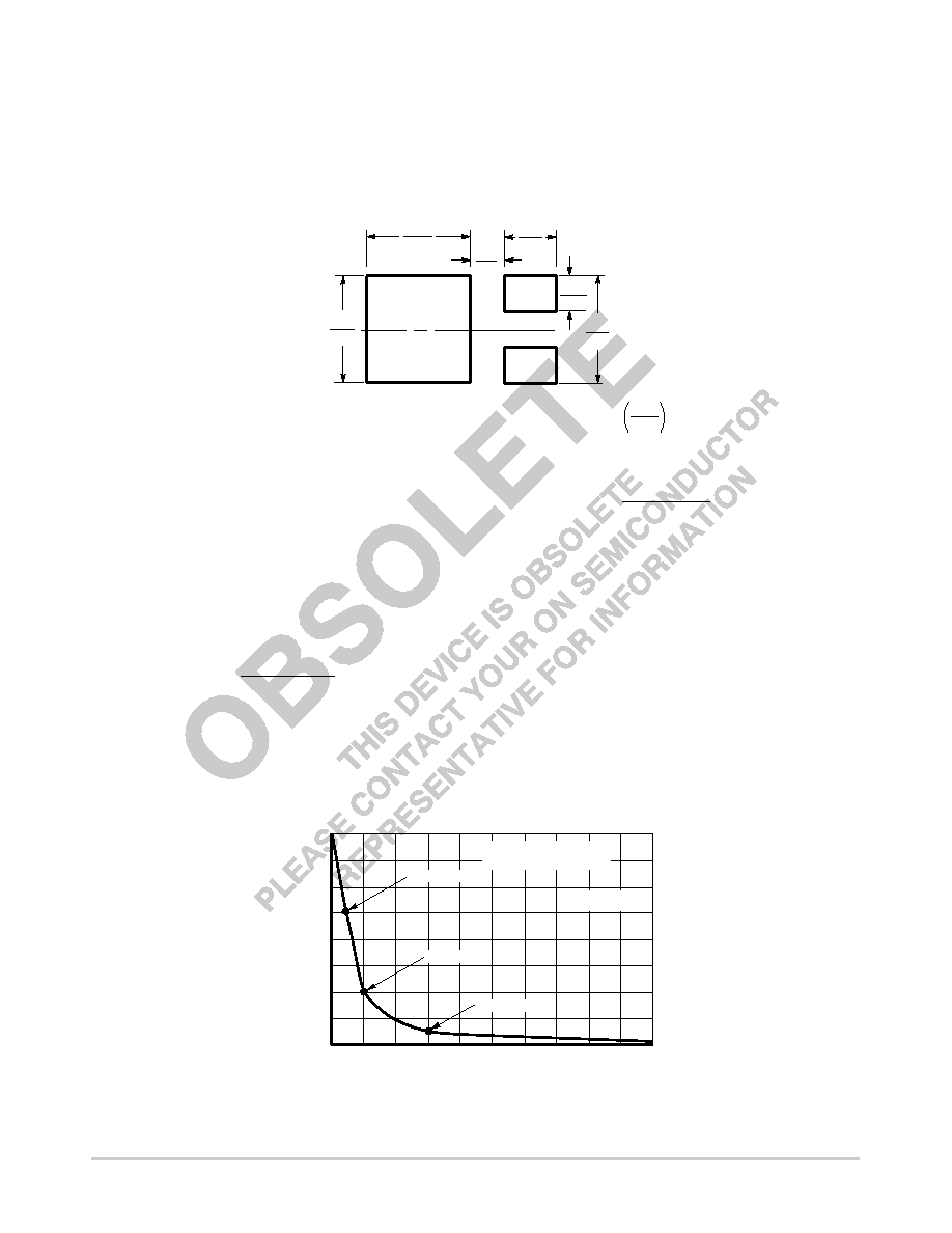
technology. For example, a graph of RθJA versus drain pad
area is shown in Figure 18.
Figure 18. Thermal Resistance versus Drain Pad
Area for the DPAK Package (Typical)
1.75 Watts
Board Material = 0.0625
″
G10/FR4, 2 oz Copper
80
100
60
40
20
10
8
6
4
2
0
3.0 Watts
5.0 Watts
TA = 25°C
A, AREA (SQUARE INCHES)
T
O
AMBIENT
(
C/W)°
R
JA
,THERMAL
RESIST
ANCE,
JUNCTION
θ
相关PDF资料 |
PDF描述 |
|---|---|
| MTD4N20E | 4 A, 200 V, 1.2 ohm, N-CHANNEL, Si, POWER, MOSFET |
| MTD4N20E1 | 4 A, 200 V, 1.2 ohm, N-CHANNEL, Si, POWER, MOSFET |
| MTD4N20E-1 | 4 A, 200 V, 1.2 ohm, N-CHANNEL, Si, POWER, MOSFET |
| MTD9N10ET4 | 9 A, 100 V, 0.25 ohm, N-CHANNEL, Si, POWER, MOSFET |
| MTD9N10E | 9 A, 100 V, 0.25 ohm, N-CHANNEL, Si, POWER, MOSFET |
相关代理商/技术参数 |
参数描述 |
|---|---|
| MTD3302T4 | 制造商:ON Semiconductor 功能描述:Trans MOSFET N-CH 30V 30A 3-Pin(2+Tab) DPAK T/R 制造商:Rochester Electronics LLC 功能描述:- Bulk 制造商:ON Semiconductor 功能描述:MOSFET Transistor, N-Channel, TO-252AA |
| MTD3610D3 | 功能描述:Photodiode 940nm 制造商:marktech optoelectronics 系列:- 包装:散装 零件状态:有效 波长:940nm 颜色 - 增强:- 频谱范围:400nm ~ 1060nm 二极管类型:- 不同 nm 时的响应度:0.45 A/W @ 660nm 响应时间:- 电压 - DC 反向(Vr)(最大值):20V 电流 - 暗(典型值):10nA 有效面积:- 视角:- 工作温度:-20°C ~ 85°C 安装类型:- 封装/外壳:- 标准包装:10 |
| MTD392 | 制造商:未知厂家 制造商全称:未知厂家 功能描述:Coaxial Transceiver Interface |
| MTD392N | 制造商:未知厂家 制造商全称:未知厂家 功能描述:Coaxial Transceiver Interface |
| MTD392V | 制造商:未知厂家 制造商全称:未知厂家 功能描述:Coaxial Transceiver Interface |
发布紧急采购,3分钟左右您将得到回复。