- 您现在的位置:买卖IC网 > Datasheet目录481 > MTP12P10G (ON Semiconductor)MOSFET P-CH 100V 12A TO220AB Datasheet资料下载
参数资料
| 型号: | MTP12P10G |
| 厂商: | ON Semiconductor |
| 文件页数: | 4/6页 |
| 文件大小: | 0K |
| 描述: | MOSFET P-CH 100V 12A TO220AB |
| 产品变化通告: | Product Obsolescence 01/Jul/2009 |
| 产品目录绘图: | MOSFET TO-220, TO-220AB |
| 标准包装: | 50 |
| FET 型: | MOSFET P 通道,金属氧化物 |
| FET 特点: | 标准 |
| 漏极至源极电压(Vdss): | 100V |
| 电流 - 连续漏极(Id) @ 25° C: | 12A |
| 开态Rds(最大)@ Id, Vgs @ 25° C: | 300 毫欧 @ 6A,10V |
| Id 时的 Vgs(th)(最大): | 4.5V @ 1mA |
| 闸电荷(Qg) @ Vgs: | 50nC @ 10V |
| 输入电容 (Ciss) @ Vds: | 920pF @ 25V |
| 功率 - 最大: | 75W |
| 安装类型: | 通孔 |
| 封装/外壳: | TO-220-3 |
| 供应商设备封装: | TO-220AB |
| 包装: | 管件 |
| 其它名称: | MTP12P10GOS |
�� �
�
�MTP12P10�
�SAFE� OPERATING� AREA� INFORMATION�
�50�
�10� m� s�
�10�
�10 ms�
�V� GS� =� 20� V�
�SINGLE� PULSE�
�1 ms�
�dc�
�0.1 ms�
�40�
�30�
�20�
�T� C� =� 25� °� C�
�1�
�R� DS(on)� LIMIT�
�PACKAGE� LIMIT�
�MTM/MTP12P06�
�10�
�MTM/MTP12P06�
�THERMAL� LIMIT� MTM/MTP12P10�
�0�
�MTM/MTP12P10�
�1�
�10�
�100�
�0�
�10�
�20�
�30�
�40�
�50�
�60�
�70�
�80�
�90�
�100�
�V� DS� ,� DRAIN?TO?SOURCE� VOLTAGE� (VOLTS)�
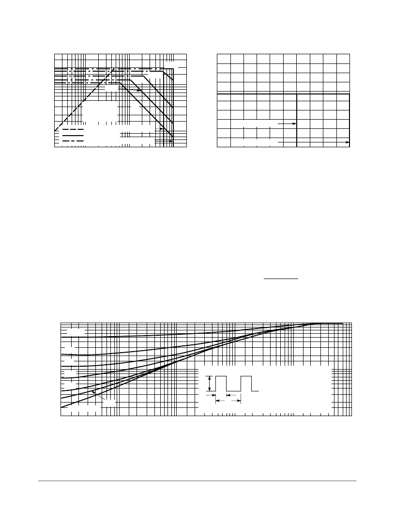
�Figure� 7.� Maximum� Rated� Forward� Biased�
�Safe� Operating� Area�
�FORWARD� BIASED� SAFE� OPERATING� AREA�
�The� FBSOA� curves� define� the� maximum� drain?to?source�
�voltage� and� drain� current� that� a� device� can� safely� handle�
�when� it� is� forward� biased,� or� when� it� is� on,� or� being� turned�
�on.� Because� these� curves� include� the� limitations� of�
�simultaneous� high� voltage� and� high� current,� up� to� the� rating�
�of� the� device,� they� are� especially� useful� to� designers� of� linear�
�systems.� The� curves� are� based� on� a� case� temperature� of� 25� °� C�
�and� a� maximum� junction� temperature� of� 150� °� C.� Limitations�
�for� repetitive� pulses� at� various� case� temperatures� can� be�
�determined� by� using� the� thermal� response� curves.� ON�
�Semiconductor� Application� Note,� AN569,� “Transient�
�Thermal� Resistance?General� Data� and� Its� Use”� provides�
�detailed� instructions.�
�1�
�V� DS� ,� DRAIN?TO?SOURCE� VOLTAGE� (VOLTS)�
�Figure� 8.� Maximum� Rated� Switching�
�Safe� Operating� Area�
�SWITCHING� SAFE� OPERATING� AREA�
�The� switching� safe� operating� area� (SOA)� of� Figure� 8� is� the�
�boundary� that� the� load� line� may� traverse� without� incurring�
�damage� to� the� MOSFET.� The� fundamental� limits� are� the�
�peak� current,� I� DM� and� the� breakdown� voltage,� V� (BR)DSS� .�
�The� switching� SOA� shown� in� Figure� 8� is� applicable� for� both�
�turn?on� and� turn?off� of� the� devices� for� switching� times� less�
�than� one� microsecond.�
�The� power� averaged� over� a� complete� switching� cycle�
�must� be� less� than:�
�T� J(max)� ? T� C�
�R� q� JC�
�0.5�
�0.3�
�D = 0.5�
�0.2�
�0.2�
�0.1�
�0.1�
�0.05�
�0.05�
�0.02�
�P� (pk)�
�R� q� JC� (t)� =� r(t)� R� q� JC�
�R� q� JC� =� 1.67� °� C/W� MAX�
�D� CURVES� APPLY� FOR� POWER�
�0.03�
�0.02�
�SINGLE PULSE�
�0.01�
�t� 1�
�t� 2�
�DUTY� CYCLE,� D� =� t� 1� /t� 2�
�PULSE� TRAIN� SHOWN�
�READ� TIME� AT� t� 1�
�T� J(pk)� ?� T� C� =� P� (pk)� R� q� JC� (t)�
�0.01�
�0.01�
�0.02�
�0.05�
�0.1�
�0.2�
�0.5�
�1�
�2� 5�
�10�
�20�
�50�
�100�
�200�
�500�
�1000�
�t,� TIME� (ms)�
�Figure� 9.� Thermal� Response�
�http://onsemi.com�
�4�
�相关PDF资料 |
PDF描述 |
|---|---|
| MTP23P06VG | MOSFET P-CH 60V 23A TO220AB |
| MTP2955V | MOSFET P-CH 60V 12A TO-220AB |
| MTP2P50E | MOSFET P-CH 500V 2A TO-220AB |
| MTP3055VL | MOSFET N-CH 60V 12A TO-220AB |
| MTP3055VL | MOSFET N-CH 60V 12A TO-220 |
相关代理商/技术参数 |
参数描述 |
|---|---|
| MTP1302 | 制造商:ON Semiconductor 功能描述:Trans MOSFET N-CH 30V 42A 3-Pin(3+Tab) TO-220 Rail 制造商:Rochester Electronics LLC 功能描述:- Bulk |
| MTP1306 | 制造商:Rochester Electronics LLC 功能描述:- Bulk 制造商:ON Semiconductor 功能描述: |
| MTP1403BQ8 | 制造商:CYSTEKEC 制造商全称:Cystech Electonics Corp. 功能描述:P-CHANNEL ENHANCEMENT MODE POWER MOSFET |
| MTP14N05L | 制造商:未知厂家 制造商全称:未知厂家 功能描述:N-Channel Enhancement MOSFET |
| MTP150 | 制造商:NELLSEMI 制造商全称:Nell Semiconductor Co., Ltd 功能描述:Three-Phase Bridge Rectifier, 150A |
发布紧急采购,3分钟左右您将得到回复。