- 您现在的位置:买卖IC网 > PDF目录268181 > NAND02GR4B2BZB1 (STMICROELECTRONICS) 128M X 16 FLASH 1.8V PROM, 35 ns, PBGA63 PDF资料下载
参数资料
| 型号: | NAND02GR4B2BZB1 |
| 厂商: | STMICROELECTRONICS |
| 元件分类: | PROM |
| 英文描述: | 128M X 16 FLASH 1.8V PROM, 35 ns, PBGA63 |
| 封装: | 9.50 X 12 MM, 1.20 MM HEIGHT, 0.80 MM PITCH, TFBGA-63 |
| 文件页数: | 14/57页 |
| 文件大小: | 887K |
| 代理商: | NAND02GR4B2BZB1 |
第1页第2页第3页第4页第5页第6页第7页第8页第9页第10页第11页第12页第13页当前第14页第15页第16页第17页第18页第19页第20页第21页第22页第23页第24页第25页第26页第27页第28页第29页第30页第31页第32页第33页第34页第35页第36页第37页第38页第39页第40页第41页第42页第43页第44页第45页第46页第47页第48页第49页第50页第51页第52页第53页第54页第55页第56页第57页
21/57
NAND01G-B, NAND02G-B, NAND04G-B, NAND08G-B
Cache Read
The Cache Read operation is used to improve the
read throughput by reading data using the Cache
Register. As soon as the user starts to read one
page, the device automatically loads the next page
into the Cache Register.
An Cache Read operation consists of three steps
(see Table 10.):
1.
One bus cycle is required to setup the Cache
Read command (the same as the standard
Read command)
2.
bus cycles are then required to input the Start
Address
3.
One bus cycle is required to issue the Cache
Read confirm command to start the P/E/R
Controller.
The Start Address must be at the beginning of a
page (Column Address = 00h, see Table 8. and
Table 9.). This allows the data to be output unin-
The Ready/Busy signal can be used to monitor the
start of the operation. During the latency period the
Ready/Busy signal goes Low, after this the Ready/
Busy signal goes High, even if the device is inter-
nally downloading page n+1.
Once the Cache Read operation has started, the
Status Register can be read using the Read Status
Register command.
During the operation, SR5 can be read, to find out
whether the internal reading is ongoing (SR5 =
‘0’), or has completed (SR5 = ‘1’), while SR6 indi-
cates whether the Cache Register is ready to
download new data.
To exit the Cache Read operation an Exit Cache
Read command must be issued (see Table 10.).
If the Exit Cache Read command is issued while
the device is internally reading page n+1, page n
will still be output, but not page n+1.
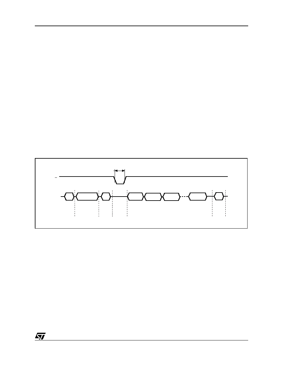
Figure 10. Cache Read Operation
I/O
RB
Address
Inputs
ai08661
00h
Read
Setup
Code
31h
Cache
Read
Confirm
Code
Busy
tBLBH1
(Read Busy time)
1st page
Data Output
2nd page
3rd page
last page
34h
Exit
Cache
Read
Code
Block N
相关PDF资料 |
PDF描述 |
|---|---|
| NCH030A3-FREQ-OUT27 | CRYSTAL OSCILLATOR, CLOCK, 1 MHz - 4 MHz, HCMOS OUTPUT |
| NTHA3JAA3-FREQ-OUT27 | CRYSTAL OSCILLATOR, CLOCK, 1 MHz - 4 MHz, HCMOS OUTPUT |
| NTHA3KC3-FREQ-OUT27 | CRYSTAL OSCILLATOR, CLOCK, 1 MHz - 4 MHz, HCMOS OUTPUT |
| NCHA80C3-FREQ1-OUT27 | CRYSTAL OSCILLATOR, CLOCK, 24 MHz - 80 MHz, HCMOS OUTPUT |
| NCHA8KB3-FREQ1-OUT27 | CRYSTAL OSCILLATOR, CLOCK, 24 MHz - 80 MHz, HCMOS OUTPUT |
相关代理商/技术参数 |
参数描述 |
|---|---|
| NAND02GR4B2CDI6 | 功能描述:闪存 NAND & S.MEDIA FLASH RoHS:否 制造商:ON Semiconductor 数据总线宽度:1 bit 存储类型:Flash 存储容量:2 MB 结构:256 K x 8 定时类型: 接口类型:SPI 访问时间: 电源电压-最大:3.6 V 电源电压-最小:2.3 V 最大工作电流:15 mA 工作温度:- 40 C to + 85 C 安装风格:SMD/SMT 封装 / 箱体: 封装:Reel |
| NAND02GR4B2CZA6E | 制造商:Micron Technology Inc 功能描述:NAND - Trays |
| NAND02GR4B2DDD6 | 制造商:Micron Technology Inc 功能描述:NAND - Gel-pak, waffle pack, wafer, diced wafer on film |
| NAND02GR4B2DE06 | 制造商:Micron Technology Inc 功能描述:NAND - Gel-pak, waffle pack, wafer, diced wafer on film |
| NAND02GR4B2DWFD | 制造商:Micron Technology Inc 功能描述:NAND - Gel-pak, waffle pack, wafer, diced wafer on film |
发布紧急采购,3分钟左右您将得到回复。