- 您现在的位置:买卖IC网 > PDF目录268181 > NAND02GR4B2BZB1 (STMICROELECTRONICS) 128M X 16 FLASH 1.8V PROM, 35 ns, PBGA63 PDF资料下载
参数资料
| 型号: | NAND02GR4B2BZB1 |
| 厂商: | STMICROELECTRONICS |
| 元件分类: | PROM |
| 英文描述: | 128M X 16 FLASH 1.8V PROM, 35 ns, PBGA63 |
| 封装: | 9.50 X 12 MM, 1.20 MM HEIGHT, 0.80 MM PITCH, TFBGA-63 |
| 文件页数: | 38/57页 |
| 文件大小: | 887K |
| 代理商: | NAND02GR4B2BZB1 |
第1页第2页第3页第4页第5页第6页第7页第8页第9页第10页第11页第12页第13页第14页第15页第16页第17页第18页第19页第20页第21页第22页第23页第24页第25页第26页第27页第28页第29页第30页第31页第32页第33页第34页第35页第36页第37页当前第38页第39页第40页第41页第42页第43页第44页第45页第46页第47页第48页第49页第50页第51页第52页第53页第54页第55页第56页第57页
43/57
NAND01G-B, NAND02G-B, NAND04G-B, NAND08G-B
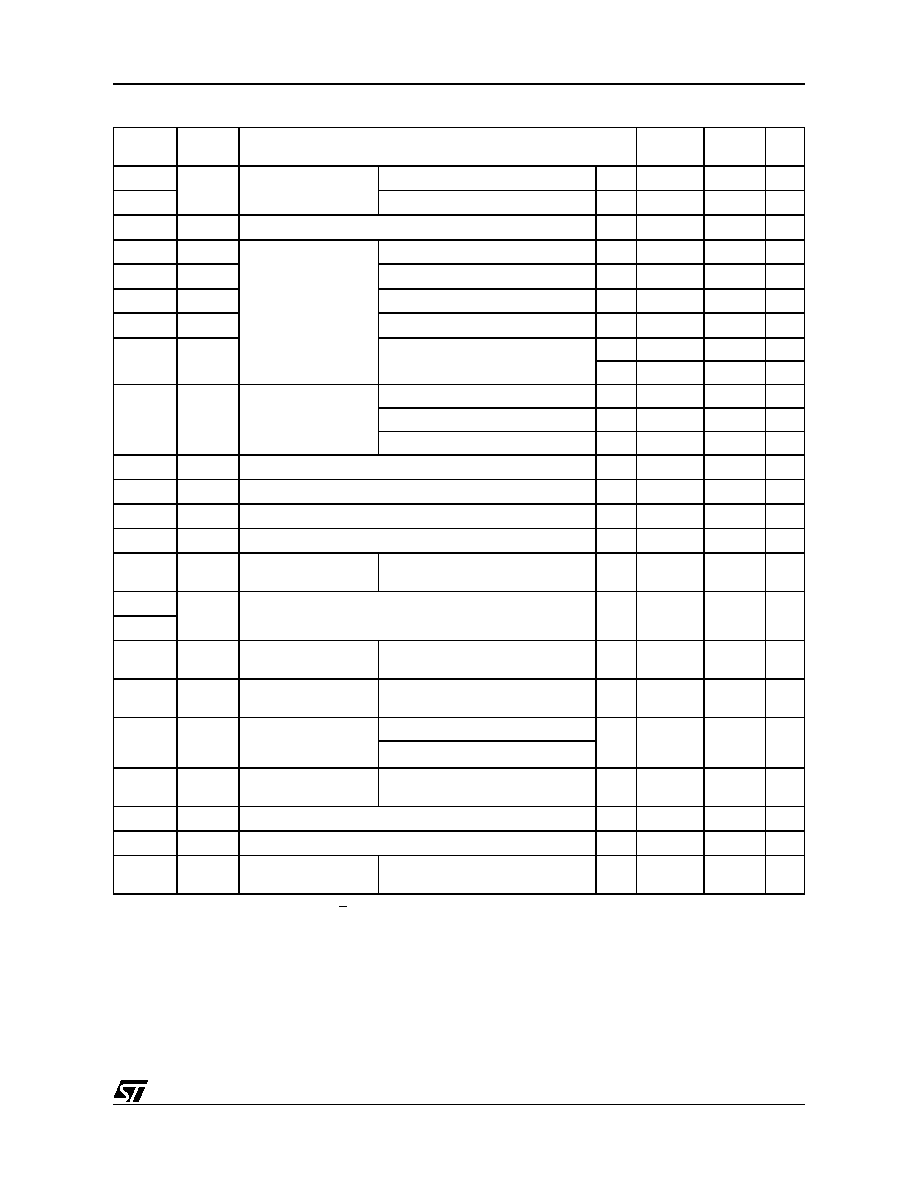
Table 25. AC Characteristics for Operations
Note: 1. The time to Ready depends on the value of the pull-up resistor tied to the Ready/Busy pin. See Figures 34, 35 and 36.
2. To break the sequential read cycle, E must be held High for longer than tEHEL.
3. ES = Electronic Signature.
Symbol
Alt.
Symbol
Parameter
1.8V
Devices
3V
Devices
Unit
tALLRL1
tAR
Address Latch Low to
Read Enable Low
Read Electronic Signature
Min
10
ns
tALLRL2
Read cycle
Min
10
ns
tBHRL
tRR
Ready/Busy High to Read Enable Low
Min
20
ns
tBLBH1
Ready/Busy Low to
Ready/Busy High
Read Busy time
Max
25
s
tBLBH2
tPROG
Program Busy time
Max
700
s
tBLBH3
tBERS
Erase Busy time
Max
3
ms
tBLBH4
Reset Busy time, during ready
Max
5
s
tBLBH5
tCBSY
Cache Busy time
Typ
3
s
Max
700
s
tWHBH1
tRST
Write Enable High to
Ready/Busy High
Reset Busy time, during read
Max
5
s
Reset Busy time, during program
Max
10
s
Reset Busy time, during erase
Max
500
s
tCLLRL
tCLR
Command Latch Low to Read Enable Low
Min
10
ns
tDZRL
tIR
Data Hi-Z to Read Enable Low
Min
0
ns
tEHQZ
tCHZ
Chip Enable High to Output Hi-Z
Max
20
ns
tELQV
tCEA
Chip Enable Low to Output Valid
Max
45
ns
tRHRL
tREH
Read Enable High to
Read Enable Low
Read Enable High Hold time
Min
20
ns
TEHQX
TOH
Chip Enable high or Read Enable high to Output Hold
Min
15
ns
TRHQX
tRLRH
tRP
Read Enable Low to
Read Enable High
Read Enable Pulse Width
Min
25
ns
tRLRL
tRC
Read Enable Low to
Read Enable Low
Read Cycle time
Min
60
50
ns
tRLQV
tREA
Read Enable Low to
Output Valid
Read Enable Access time
Max
35
ns
Read ES Access time(3)
tWHBH
tR
Write Enable High to
Ready/Busy High
Read Busy time
Max
25
s
tWHBL
tWB
Write Enable High to Ready/Busy Low
Max
100
ns
tWHRL
tWHR
Write Enable High to Read Enable Low
Min
60
ns
tWLWL
tWC
Write Enable Low to
Write Enable Low
Write Cycle time
Min
60
50
ns
相关PDF资料 |
PDF描述 |
|---|---|
| NCH030A3-FREQ-OUT27 | CRYSTAL OSCILLATOR, CLOCK, 1 MHz - 4 MHz, HCMOS OUTPUT |
| NTHA3JAA3-FREQ-OUT27 | CRYSTAL OSCILLATOR, CLOCK, 1 MHz - 4 MHz, HCMOS OUTPUT |
| NTHA3KC3-FREQ-OUT27 | CRYSTAL OSCILLATOR, CLOCK, 1 MHz - 4 MHz, HCMOS OUTPUT |
| NCHA80C3-FREQ1-OUT27 | CRYSTAL OSCILLATOR, CLOCK, 24 MHz - 80 MHz, HCMOS OUTPUT |
| NCHA8KB3-FREQ1-OUT27 | CRYSTAL OSCILLATOR, CLOCK, 24 MHz - 80 MHz, HCMOS OUTPUT |
相关代理商/技术参数 |
参数描述 |
|---|---|
| NAND02GR4B2CDI6 | 功能描述:闪存 NAND & S.MEDIA FLASH RoHS:否 制造商:ON Semiconductor 数据总线宽度:1 bit 存储类型:Flash 存储容量:2 MB 结构:256 K x 8 定时类型: 接口类型:SPI 访问时间: 电源电压-最大:3.6 V 电源电压-最小:2.3 V 最大工作电流:15 mA 工作温度:- 40 C to + 85 C 安装风格:SMD/SMT 封装 / 箱体: 封装:Reel |
| NAND02GR4B2CZA6E | 制造商:Micron Technology Inc 功能描述:NAND - Trays |
| NAND02GR4B2DDD6 | 制造商:Micron Technology Inc 功能描述:NAND - Gel-pak, waffle pack, wafer, diced wafer on film |
| NAND02GR4B2DE06 | 制造商:Micron Technology Inc 功能描述:NAND - Gel-pak, waffle pack, wafer, diced wafer on film |
| NAND02GR4B2DWFD | 制造商:Micron Technology Inc 功能描述:NAND - Gel-pak, waffle pack, wafer, diced wafer on film |
发布紧急采购,3分钟左右您将得到回复。