- 您现在的位置:买卖IC网 > PDF目录189002 > NAND512R3A0CV1F (STMICROELECTRONICS) 64M X 8 FLASH 1.8V PROM, 35 ns, PDSO48 PDF资料下载
参数资料
| 型号: | NAND512R3A0CV1F |
| 厂商: | STMICROELECTRONICS |
| 元件分类: | PROM |
| 英文描述: | 64M X 8 FLASH 1.8V PROM, 35 ns, PDSO48 |
| 封装: | 12 X 17 MM, 0.65 MM HEIGHT, ROHS COMPLIANT, PLASTIC, USOP-48 |
| 文件页数: | 7/57页 |
| 文件大小: | 916K |
| 代理商: | NAND512R3A0CV1F |
第1页第2页第3页第4页第5页第6页当前第7页第8页第9页第10页第11页第12页第13页第14页第15页第16页第17页第18页第19页第20页第21页第22页第23页第24页第25页第26页第27页第28页第29页第30页第31页第32页第33页第34页第35页第36页第37页第38页第39页第40页第41页第42页第43页第44页第45页第46页第47页第48页第49页第50页第51页第52页第53页第54页第55页第56页第57页
15/57
NAND128-A, NAND256-A, NAND512-A, NAND01G-A
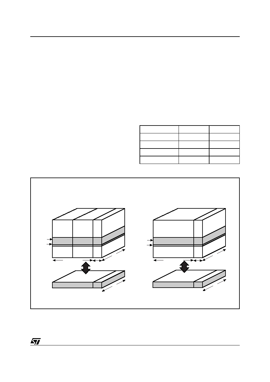
MEMORY ARRAY ORGANIZATION
The memory array is made up of NAND structures
where 16 cells are connected in series.
The memory array is organized in blocks where
each block contains 32 pages. The array is split
into two areas, the main area and the spare area.
The main area of the array is used to store data
whereas the spare area is typically used to store
Error correction Codes, software flags or Bad
Block identification.
In x8 devices the pages are split into a main area
with two half pages of 256 Bytes each and a spare
area of 16 Bytes. In the x16 devices the pages are
split into a 256 Word main area and an 8 Word
spare area. Refer to Figure 10., Memory Array Or-
Bad Blocks
The NAND Flash 528 Byte/ 264 Word Page devic-
es may contain Bad Blocks, that is blocks that con-
tain one or more invalid bits whose reliability is not
guaranteed. Additional Bad Blocks may develop
during the lifetime of the device.
The Bad Block Information is written prior to ship-
ping (refer to Bad Block Management section for
more details).
Table 4. shows the minimum number of valid
blocks in each device. The values shown include
both the Bad Blocks that are present when the de-
vice is shipped and the Bad Blocks that could de-
velop later on.
These blocks need to be managed using Bad
Blocks Management, Block Replacement or Error
Correction Codes (refer to SOFTWARE ALGO-
RITHMS section).
Table 4. Valid Blocks
Figure 10. Memory Array Organization
Density of Device
Min
Max
1Gbit
8032
8192
512Mbits
4016
4096
256Mbits
2008
2048
128Mbits
1004
1024
AI07587
Block = 32 Pages
Page = 528 Bytes (512+16)
512 Bytes
Spare
Area
2nd half Page
(256 bytes)
16
Bytes
Block
8 bits
16
Bytes
8 bits
Page
Page Buffer, 512 Bytes
1st half Page
(256 bytes)
Block = 32 Pages
Page = 264 Words (256+8)
256 Words
Spare
Area
Main Area
8
Words
16 bits
8
Words
16 bits
Page Buffer, 264 Words
Block
Page
x8 DEVICES
x16 DEVICES
相关PDF资料 |
PDF描述 |
|---|---|
| NAND512R3A0AN6E | 64M X 8 FLASH 1.8V PROM, 35 ns, PDSO48 |
| NAND512R3A0AZA6E | 64M X 8 FLASH 1.8V PROM, 35 ns, PBGA63 |
| NAND512R3A2AN6T | 64M X 8 FLASH 1.8V PROM, 35 ns, PDSO48 |
| NAND512R3A2CN1F | 64M X 8 FLASH 1.8V PROM, 35 ns, PDSO48 |
| NAND512R3A2AV1E | 64M X 8 FLASH 1.8V PROM, 35 ns, PDSO48 |
相关代理商/技术参数 |
参数描述 |
|---|---|
| NAND512R3A2AZA6E | 功能描述:IC FLASH 512MBIT 55VFBGA RoHS:否 类别:集成电路 (IC) >> 存储器 系列:- 标准包装:576 系列:- 格式 - 存储器:闪存 存储器类型:闪存 - NAND 存储容量:512M(64M x 8) 速度:- 接口:并联 电源电压:2.7 V ~ 3.6 V 工作温度:-40°C ~ 85°C 封装/外壳:48-TFSOP(0.724",18.40mm 宽) 供应商设备封装:48-TSOP 包装:托盘 其它名称:497-5040 |
| NAND512R3A2BZA6E | 功能描述:闪存 128Mbit-1Gbit 1.8/3V RoHS:否 制造商:ON Semiconductor 数据总线宽度:1 bit 存储类型:Flash 存储容量:2 MB 结构:256 K x 8 定时类型: 接口类型:SPI 访问时间: 电源电压-最大:3.6 V 电源电压-最小:2.3 V 最大工作电流:15 mA 工作温度:- 40 C to + 85 C 安装风格:SMD/SMT 封装 / 箱体: 封装:Reel |
| NAND512R3A2CZA6E | 功能描述:IC FLASH 512MBIT 63VFBGA RoHS:是 类别:集成电路 (IC) >> 存储器 系列:- 产品变化通告:Product Discontinuation 26/Apr/2010 标准包装:136 系列:- 格式 - 存储器:RAM 存储器类型:SRAM - 同步,DDR II 存储容量:18M(1M x 18) 速度:200MHz 接口:并联 电源电压:1.7 V ~ 1.9 V 工作温度:0°C ~ 70°C 封装/外壳:165-TBGA 供应商设备封装:165-CABGA(13x15) 包装:托盘 其它名称:71P71804S200BQ |
| NAND512R3A2CZA6F | 制造商:Micron Technology Inc 功能描述:SLC NAND Flash Parallel 1.8V 512Mbit 64M x 8bit 15us 63-Pin VFBGA T/R |
| NAND512R3A2DDI6 | 制造商:Micron Technology Inc 功能描述:NAND - Gel-pak, waffle pack, wafer, diced wafer on film |
发布紧急采购,3分钟左右您将得到回复。