- 您现在的位置:买卖IC网 > PDF目录1956 > NCN6004AFTBR2G (ON Semiconductor)IC INTERFACE SAM/SIM DUAL 48TQFP PDF资料下载
参数资料
| 型号: | NCN6004AFTBR2G |
| 厂商: | ON Semiconductor |
| 文件页数: | 15/40页 |
| 文件大小: | 0K |
| 描述: | IC INTERFACE SAM/SIM DUAL 48TQFP |
| 标准包装: | 1 |
| 应用: | PC,PDA |
| 接口: | 微控制器 |
| 电源电压: | 1.8 V ~ 5.5 V |
| 封装/外壳: | 48-TQFP 裸露焊盘 |
| 供应商设备封装: | 48-TQFP(7x7) |
| 包装: | 标准包装 |
| 安装类型: | 表面贴装 |
| 其它名称: | NCN6004AFTBR2GOSDKR |
第1页第2页第3页第4页第5页第6页第7页第8页第9页第10页第11页第12页第13页第14页当前第15页第16页第17页第18页第19页第20页第21页第22页第23页第24页第25页第26页第27页第28页第29页第30页第31页第32页第33页第34页第35页第36页第37页第38页第39页第40页
NCN6004A
http://onsemi.com
22
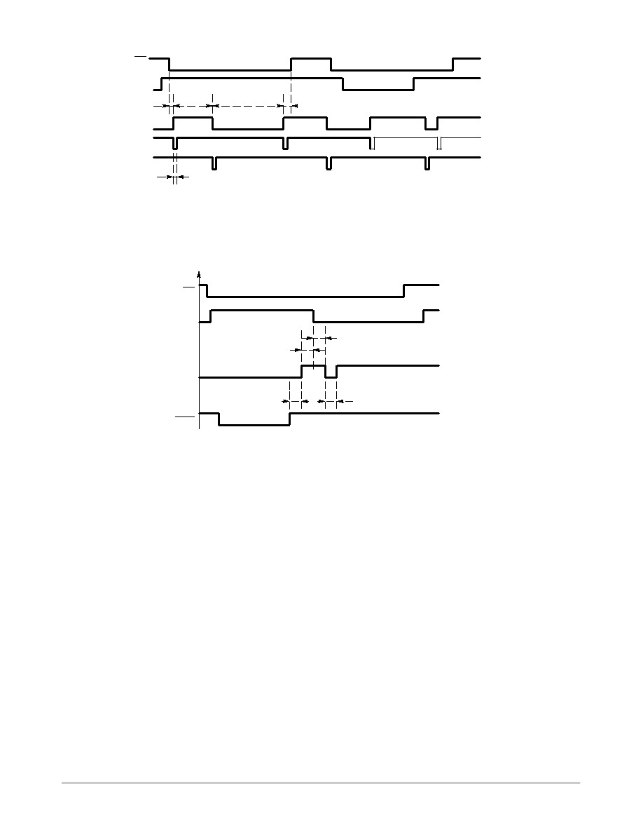
PWR_ON
tpwrhold
tpwrlow
CARD_SEL
SET
RESET
tpwrpre
tpwrset
tpwrp
NOTE:
tpwrset: This delay is necessary to latch–up the PWR_ON condition
and does not represent the CRD_VCC output voltage rise time.
tpwrlow: This delay includes the internal ISO78163 power down
sequence to make sure the DC/DC converter is fully deactivated.
Figure 13. Power On Sequence Timings
CS
PWR_ON
tpgmdly
CARD_SEL
tcseldly
tpwrw
Programming
Chip Selected
tpwrhold
NOTE:
tpwrw: This delay represents the minimum pulse width needed
to write the PWR_ON status into the associated DC/DC latch
Figure 14. Power On and CARD_SEL Sequence Timings
Sequence
CS
PGM
DC/DC CONVERTER
The power conversion is carried out either in step up or
step down mode. The operation is fully automatic and,
beside the output voltage programming, does not need any
further adjustments.
The simplified DC/DC converter, given in Figure 15, is
based on a full bridge structure capable to handle either step
up or step down power supply using an external inductor.
This structure brings the capability to operate from a wide
range of input voltage, while providing the accurate 1.80 V,
3.0 V or 5.0 V requested by the smart cards. Beside the
accuracy, the major aim of this structure is the high
efficiency necessary to save energy taken from the battery.
On the other hand, using two independent converters
provides a high flexibility and prevent a total system crash
in the event of a failure on one of the card connected to the
interface.
OPERATION
NOTE:
Described operation makes reference to
CARD_A and can be applied to CARD_B.
The system operates with a two cycles concept:
1. Cycle 1: Q15 and Q4 are switched ON and the
inductor L1 is charged by the energy supplied by
the external battery. During this phase, the pairs
Q1/Q16 and Q2/Q3 are switched OFF.
The current flowing into the two MOSFET Q1 and
Q4 is internally monitored and will be switched OFF
when the Ipeak value (depending upon the
programmed output voltage value) is reached. At
this point, Cycle 1 is completed and Cycle 2 takes
place. The ON time is a function of the battery
voltage and the value of the inductor network (L and
Zr) connected across pins 26/27 and 34/35.
A 4
ms time out structure makes sure the system does
run in a continuous Cycle 1 loop.
2. Cycle 2: Q1 and Q16 are switched ON and the
energy stored into the inductor L1 is dumped into
the external load through Q16. During this phase,
the pair Q15/Q4 and the pair Q2/Q3 are switched
OFF.
The current flow period is constant (900 ns typical)
and Cycle 1 repeats after this time if the CRD_VCC
voltage is below the specified value.
相关PDF资料 |
PDF描述 |
|---|---|
| NCN6804MNR2G | IC SMART CARD DUAL W/SPI 32-QFN |
| NCN7200MTTWG | IC MUX/DEMUX OCTAL 1X2 42WQFN |
| NCN8024DTBR2G | SMART CARD IC 5V/3V TSSOP |
| NCN8024RDWR2G | IC SMART CARD IC2 28SOIC |
| NCN8025MTTBG | IC SMART CARD I2C 16-QFN |
相关代理商/技术参数 |
参数描述 |
|---|---|
| NCN6010 | 制造商:ONSEMI 制造商全称:ON Semiconductor 功能描述:SIM Card Supply and Level Shifter |
| NCN6010/D | 制造商:ONSEMI 制造商全称:ON Semiconductor 功能描述:SIM Card Supply and Level Shifter |
| NCN6010_06 | 制造商:ONSEMI 制造商全称:ON Semiconductor 功能描述:SIM Card Supply and Level Shifter |
| NCN6010D | 制造商:ONSEMI 制造商全称:ON Semiconductor 功能描述:SIM Card Supply and Level Shifter |
| NCN6010DTB | 功能描述:转换 - 电压电平 2.7V Sim Card RoHS:否 制造商:Micrel 类型:CML/LVDS/LVPECL to LVCMOS/LVTTL 传播延迟时间:1.9 ns 电源电流:14 mA 电源电压-最大:3.6 V 电源电压-最小:3 V 最大工作温度:+ 85 C 安装风格:SMD/SMT 封装 / 箱体:MLF-8 |
发布紧急采购,3分钟左右您将得到回复。