- 您现在的位置:买卖IC网 > PDF目录1956 > NCN6004AFTBR2G (ON Semiconductor)IC INTERFACE SAM/SIM DUAL 48TQFP PDF资料下载
参数资料
| 型号: | NCN6004AFTBR2G |
| 厂商: | ON Semiconductor |
| 文件页数: | 24/40页 |
| 文件大小: | 0K |
| 描述: | IC INTERFACE SAM/SIM DUAL 48TQFP |
| 标准包装: | 1 |
| 应用: | PC,PDA |
| 接口: | 微控制器 |
| 电源电压: | 1.8 V ~ 5.5 V |
| 封装/外壳: | 48-TQFP 裸露焊盘 |
| 供应商设备封装: | 48-TQFP(7x7) |
| 包装: | 标准包装 |
| 安装类型: | 表面贴装 |
| 其它名称: | NCN6004AFTBR2GOSDKR |
第1页第2页第3页第4页第5页第6页第7页第8页第9页第10页第11页第12页第13页第14页第15页第16页第17页第18页第19页第20页第21页第22页第23页当前第24页第25页第26页第27页第28页第29页第30页第31页第32页第33页第34页第35页第36页第37页第38页第39页第40页
NCN6004A
http://onsemi.com
30
The input clock A and B can be re routed to either
CRD_CLK_A or CRD_CLK_B output pins by using the
clock signals can have any frequency value necessary to
handle a given type of card (asynchronous or synchronous).
These clock signals can be multiplexed at any time, but the
system must be locked in a safe state prior to make such a
change. In particular, the designer must make sure that A and
B cards can support such a hot change prior to change the
related clocks.
Table 7. Programming Clock Routing
STATE
CS
PGM
A3
A2
A1
A0
CARD_SEL
CRD_CLK_A
CRD_CLK_B
0E
0
1
0
1
CLK_D_A
Default
0F
0
1
CLK_D_B
0E
0
1
0
CLK_D_B
Default
0F
0
1
0
CLK_D_A
On the other hand, the slope of the CRD_CLK_x signal
can be set to either FAST or SLOW, depending upon the
frequency of the output clock. This selection is achieved by
programming the chip according to Table 8.
Table 8. Output Clock Slope Selection
STATE
CS
PGM
A3
A2
A1
A0
CARD_SEL
CLOCK SLOPE
$03
0
1
SLOW
Default
$0B
0
1
0
1
FAST
$03
0
1
0
SLOW
Default
$0B
0
1
0
1
0
FAST
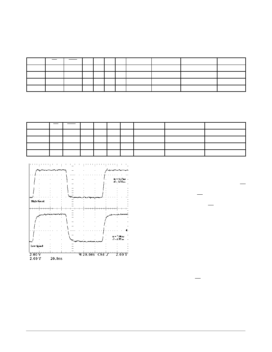
Figure 30. Typical Rise and Fall Time in Fast and
Slow Operating Mode
PARALLEL OPERATION
When two or more NCN6004A parts operate in parallel on
a common digital bus, the Chip Select pin allows the
selection of one chip from the bank of the paralleled devices.
Of course, the external MPU shall provide one unique CS
line for each of the NCN6004A considered interface. When
a given interface is selected by CS = L, all the logic inputs
becomes active, the chip can be programmed or/and the
external card can be accessed. When CS = H, all the input
logic pins are in the high impedance state, thus leaving the
bus available for other purpose.
The pull up resistors connected on each logic input lines on
the MPU side (see block diagram in Figure 30), can be either
activated (connected to VCC) or disconnected, depending
upon the logic state present at EN_RPU, pin 45. When these
resistors are disconnected, it is the system responsibility to
set up the external pull up resistors according to the
application’s requirements.
When the device operates in the multiplexed mode
(MUX_MODE = High), the internal card #B pull up
resistors are connected to VCC, regardless of the EN_RPU
logic state.
On the other hand, when CS = H, the CRD_IO and
CRD_RST hold the previous I/O and RESET logic state, the
CRD_CLK being either active or stopped and the
CRD_VCC output voltage will maintain is previous value,
according to the programmed state forced by the MPU.
相关PDF资料 |
PDF描述 |
|---|---|
| NCN6804MNR2G | IC SMART CARD DUAL W/SPI 32-QFN |
| NCN7200MTTWG | IC MUX/DEMUX OCTAL 1X2 42WQFN |
| NCN8024DTBR2G | SMART CARD IC 5V/3V TSSOP |
| NCN8024RDWR2G | IC SMART CARD IC2 28SOIC |
| NCN8025MTTBG | IC SMART CARD I2C 16-QFN |
相关代理商/技术参数 |
参数描述 |
|---|---|
| NCN6010 | 制造商:ONSEMI 制造商全称:ON Semiconductor 功能描述:SIM Card Supply and Level Shifter |
| NCN6010/D | 制造商:ONSEMI 制造商全称:ON Semiconductor 功能描述:SIM Card Supply and Level Shifter |
| NCN6010_06 | 制造商:ONSEMI 制造商全称:ON Semiconductor 功能描述:SIM Card Supply and Level Shifter |
| NCN6010D | 制造商:ONSEMI 制造商全称:ON Semiconductor 功能描述:SIM Card Supply and Level Shifter |
| NCN6010DTB | 功能描述:转换 - 电压电平 2.7V Sim Card RoHS:否 制造商:Micrel 类型:CML/LVDS/LVPECL to LVCMOS/LVTTL 传播延迟时间:1.9 ns 电源电流:14 mA 电源电压-最大:3.6 V 电源电压-最小:3 V 最大工作温度:+ 85 C 安装风格:SMD/SMT 封装 / 箱体:MLF-8 |
发布紧急采购,3分钟左右您将得到回复。