- 您现在的位置:买卖IC网 > PDF目录1956 > NCN6004AFTBR2G (ON Semiconductor)IC INTERFACE SAM/SIM DUAL 48TQFP PDF资料下载
参数资料
| 型号: | NCN6004AFTBR2G |
| 厂商: | ON Semiconductor |
| 文件页数: | 39/40页 |
| 文件大小: | 0K |
| 描述: | IC INTERFACE SAM/SIM DUAL 48TQFP |
| 标准包装: | 1 |
| 应用: | PC,PDA |
| 接口: | 微控制器 |
| 电源电压: | 1.8 V ~ 5.5 V |
| 封装/外壳: | 48-TQFP 裸露焊盘 |
| 供应商设备封装: | 48-TQFP(7x7) |
| 包装: | 标准包装 |
| 安装类型: | 表面贴装 |
| 其它名称: | NCN6004AFTBR2GOSDKR |
第1页第2页第3页第4页第5页第6页第7页第8页第9页第10页第11页第12页第13页第14页第15页第16页第17页第18页第19页第20页第21页第22页第23页第24页第25页第26页第27页第28页第29页第30页第31页第32页第33页第34页第35页第36页第37页第38页当前第39页第40页
NCN6004A
http://onsemi.com
8
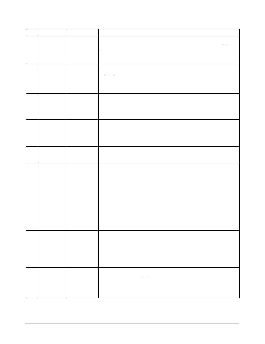
PIN DESCRIPTION (continued)
Pin
Description
Type
Symbol
39
CRD_C4_B
OUTPUT
This pin controls the card #B C4 contact, according to the ISO specification. A builtin level
shifter is used to adapt the card and the MCU, regardless of the power supply voltage of
each signals. The signal present at this pin is latched upon either CARD_SEL or CS or
PGM positive going transient and resume to a transparent mode when card #B is selected.
The pin is hardwired to zero, the bias being provided by the VCC supply, when either the
VCC voltage drops below 2.7 V, or during the CRD_VCC_B startup time.
40
CRD_C8_B
OUTPUT
This pin controls the card #B C8 contact, according to the ISO specification. A builtin
level shifter is used to adapt the card and the MCU, regardless of the power supply
voltage of each signals. The signal present at this pin is latched upon either CARD_SEL
or CS or PGM positive going transient and resume to a transparent mode when card #B
is selected.
The pin is hardwired to zero, the bias being provided by the VCC supply, when either the
VCC voltage drops below 2.7 V, or during the CRD_VCC_B startup time.
41
CRD_DET_B
INPUT
This pin senses the signal coming from the external smart card connector to detect the
presence of card #B. The polarity of the signal is programmable as Normally Open or
Normally Close switch. The logic signal will be activated when the level is either Low or
High, with respect to the polarity defined previously. By default, the input is Normally
Open. A builtin circuit prevents uncontrolled short pulses to generate an INT signal. The
digital filter eliminates pulse width below 50
ms.
42
ANLG_VCC
POWER
This pin is connected to the positive external power supply. The device sustains any
voltage from +2.7 V to +5.5 V. This voltage supplies the NCN6004A internal Analog and
Logic circuits. A high quality capacitor must be connected across this pin and
ANLG_GND, 10
mF/6 V is recommended. A set of extra pins (28 and 33) are provided to
connect the power supply to the internal DC/DC converter.
Note: The voltage present at pin 28 and 33 must be equal to the voltage present at pin 42
43
ANLG_GND
GROUND
This pin is the ground reference for both analog and digital signals and must be
connected to the system Ground. Care must be observed to provide a copper PCB layout
designed to avoid small signals and power transients sharing the same track. Good high
frequency techniques are strongly recommended.
44
MUX_MODE
INPUT
This pin selects the mode of operation of the card signals from the MPU side. When
MUX_MODE = Low, all the card signals are fully demultiplexed and data transfers can
take place with both cards simultaneously. On top of that, both cards can be accessed
during the programming sequence, assuming the external microcontroller is capable to
run multi tasks software.
When MUX_MODE = High, all the card signals are multiplexed and the communications
with the cards shall take place in a sequential mode. The card is selected by setting
CARD_SEL high or Low. The internal logic will disable the CARD_B inputs and use
CARD_SEL inputs as a single channel to controls both output smart cards sequentially
when MUX_MODE = H.
Moreover, when MUX_MODE = High, all the B channel
mP dedicated pins, except
CLOCK_IN_B, pin 15, are forced to a high level by means of internal pull up resistors. It
is not necessary to connect these pins (16, 17, 18 and 19) to an external bias voltage, but
it is mandatory to avoid any connections to ground. On the other hand, in this case the
internal pull up resistor connected across I/O_A, pin 9 and VCC is automatically
disconnected to avoid a current overload on the I/O line.
45
EN_RPU
INPUT
This pin provides a logic input to valid or not the internal pullup resistors connected
across each I/O, RESET, C4 and C8 lines and ANLG_VCC.
When EN_RPU = High, the pull up resistors are connected
When EN_RPU = Low, the pull up resistors are disconnected and it is up to the designer
to set up the external resistor to cope with the ISO/EMV specifications.
The logic signal must be set up prior to apply the ANLG_VCC supply. Once the logic
mode has been acknowledged by the internal Power On reset, it cannot be changed until
a new startup sequence is launched.
46
STATUS
OUTPUT
This pin provides a logic state related to the card [A or B] insertion, the VCC_OK, the
CRD_VCC value and the current overflow powered to either card [A or B]. The internal
register can be read when PGM = High. The logic level is forced to High when the input
voltage drops below the Vbat min (2.0 V), thus reducing the stand by current, assuming
the STATUS pin is not pulled down externally.
The associated pullup resistor is either connected to VCC (EN_RPU = H) or disconnected
when EN_RPU = Low.
相关PDF资料 |
PDF描述 |
|---|---|
| NCN6804MNR2G | IC SMART CARD DUAL W/SPI 32-QFN |
| NCN7200MTTWG | IC MUX/DEMUX OCTAL 1X2 42WQFN |
| NCN8024DTBR2G | SMART CARD IC 5V/3V TSSOP |
| NCN8024RDWR2G | IC SMART CARD IC2 28SOIC |
| NCN8025MTTBG | IC SMART CARD I2C 16-QFN |
相关代理商/技术参数 |
参数描述 |
|---|---|
| NCN6010 | 制造商:ONSEMI 制造商全称:ON Semiconductor 功能描述:SIM Card Supply and Level Shifter |
| NCN6010/D | 制造商:ONSEMI 制造商全称:ON Semiconductor 功能描述:SIM Card Supply and Level Shifter |
| NCN6010_06 | 制造商:ONSEMI 制造商全称:ON Semiconductor 功能描述:SIM Card Supply and Level Shifter |
| NCN6010D | 制造商:ONSEMI 制造商全称:ON Semiconductor 功能描述:SIM Card Supply and Level Shifter |
| NCN6010DTB | 功能描述:转换 - 电压电平 2.7V Sim Card RoHS:否 制造商:Micrel 类型:CML/LVDS/LVPECL to LVCMOS/LVTTL 传播延迟时间:1.9 ns 电源电流:14 mA 电源电压-最大:3.6 V 电源电压-最小:3 V 最大工作温度:+ 85 C 安装风格:SMD/SMT 封装 / 箱体:MLF-8 |
发布紧急采购,3分钟左右您将得到回复。