- 您现在的位置:买卖IC网 > Datasheet目录345 > NCP1910GEVB (ON Semiconductor)BOARD DEMO NCP1910DEMO-B-TLS Datasheet资料下载
参数资料
| 型号: | NCP1910GEVB |
| 厂商: | ON Semiconductor |
| 文件页数: | 2/37页 |
| 文件大小: | 0K |
| 描述: | BOARD DEMO NCP1910DEMO-B-TLS |
| 设计资源: | NCP1910 Schematic NCP1910GEVB BOM |
| 标准包装: | 1 |
| 主要目的: | DC/DC,步降 |
| 输出及类型: | 1,非隔离 |
| 输出电压: | 最低可调至 0.8V |
| 电流 - 输出: | 3A |
| 输入电压: | 3 ~ 5.5 V |
| 稳压器拓扑结构: | 降压 |
| 频率 - 开关: | 1MHz |
| 板类型: | 完全填充 |
| 已供物品: | 板 |
| 已用 IC / 零件: | NCP1910 |
| 其它名称: | NCP1910GEVBOS |
第1页当前第2页第3页第4页第5页第6页第7页第8页第9页第10页第11页第12页第13页第14页第15页第16页第17页第18页第19页第20页第21页第22页第23页第24页第25页第26页第27页第28页第29页第30页第31页第32页第33页第34页第35页第36页第37页
�� �
�
�NCP1910�
�SS�
�Rt�
�PG� out�
�ON/OFF�
�BO� adj.�
�Vref�
�PG� adj.�
�OVP2�
�FB�
�VCTRL�
�VM�
�LBO�
�1�
�24�
�Vboot�
�MU�
�Bridge�
�ML�
�V� CC�
�DRV�
�GND/PGND�
�Skip/AGND�
�CS/FF�
�CS�
�Fold�
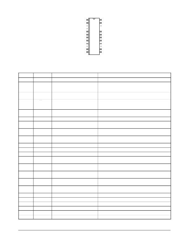
�Figure� 1.� Pin� Connections�
�PIN� DESCRIPTION�
�Pin� N� 5�
�1�
�2�
�3�
�4�
�5�
�6�
�7�
�8�
�9�
�10�
�11�
�12�
�13�
�14�
�15�
�16�
�17�
�18�
�19�
�20�
�22�
�23�
�24�
�Pin� Name�
�SS�
�Rt�
�PG� out�
�on/off�
�BO� adj.�
�Vref�
�PG� adj.�
�OVP2�
�FB�
�V� CTRL�
�V� M�
�LBO�
�Fold�
�CS�
�CS/FF�
�Skip/AGND�
�GND/PGND�
�DRV�
�V� CC�
�ML�
�Bridge�
�MU�
�V� boot�
�Function�
�Soft� ?� start�
�The� LLC� feedback� pin�
�The� open� ?� collector� power� good� signal�
�Remote� control�
�Brown� ?� out� adjustment�
�The� 5� V� reference� pin�
�The� power� good� trip� level�
�Redundant� OVP�
�PFC� feedback�
�PFC� Error� amplifier� output�
�PFC� current� amplifier� output�
�PFC� line� input� voltage� sensing�
�PFC� fold� back�
�PFC� current� sense�
�Fast� ?� fault� input�
�Skip� (B)/AGND� (A)�
�GND� (B)/PGND� (A)�
�PFC� drive� signal�
�The� controller� supply�
�Lower� ?� side� MOSFET�
�Half� ?� bridge�
�Upper� ?� side� MOSFET�
�Bootstrapped� Vcc�
�Pin� Description�
�A� capacitor� to� ground� sets� the� LLC� soft� ?� start� duration�
�A� resistive� arrangement� sets� the� maximum� and� minimum�
�switching� frequencies� with� opto� coupler� ?� based� feedback�
�capabilities.�
�This� pin� is� low� when� V� bulk� is� ok,� opens� when� V� bulk� passes�
�below� a� level� adjusted� by� PGadj� pin.�
�When� pulled� low,� the� circuit� operates:� the� PFC� starts� first� and�
�once� FB� is� in� regulation,� the� LLC� is� authorized� to� work.� When�
�left� open,� the� controller� is� in� idle� mode.�
�This� pin� sets� the� on� and� off� levels� for� the� PFC� powering� the�
�LLC� converter�
�This� pin� delivers� a� stable� voltage� for� threshold� adjustments�
�From� the� Vref� pin,� a� dc� level� sets� the� trip� point� for� the� PFC�
�bulk� voltage� at� which� the� PG� out� signal� is� down.�
�A� fully� latched� OVP� monitoring� the� PFC� bulk� independently�
�from� FB� pin.�
�Monitors� the� boost� bulk� voltage� and� regulates� it.� It� also� serves�
�as� a� quick� auto� ?� recovery� OVP�
�PFC� error� amplifier� compensation� pin�
�A� resistor� to� ground� sets� the� maximum� power� level�
�Line� feed� forward� and� PFC� brown� ?� out�
�This� pin� selects� the� power� level� at� which� the� frequency� starts�
�to� reduce� gradually.�
�This� pin� senses� the� inductor� current� and� also� programs� the�
�maximum� sense� voltage� excursion�
�When� pulled� above� 1� V,� the� LLC� stops� and� re� ?� starts� via� a� full�
�soft� ?� start� sequence.�
�This� pin� is� either� used� as� the� analog� GND� for� the� signal� circuit�
�(A)� or� for� skip� operation� (B).�
�The� controller� ground� for� the� driving� loop� (A)� or� the� lump�
�ground� pin� for� all� circuits� (B)�
�The� driving� signal� to� the� PFC� power� MOSFET�
�The� power� supply� pin� for� the� controller,� 20� V� max.�
�Drive� signal� for� the� lower� side� half� ?� bridge� MOSFET�
�This� pin� connects� to� the� LLC� half� ?� bridge�
�Drive� signal� for� the� upper� side� half� ?� bridge� MOSFET�
�The� bootstrapped� V� CC� for� the� floating� driver�
�http://onsemi.com�
�2�
�相关PDF资料 |
PDF描述 |
|---|---|
| NCP3418BMNR2G | IC MOSFET DRIVER DUAL 12V 10-DFN |
| NCP3418DR2 | IC MOSFET DRIVER DUAL 12V 8-SOIC |
| NCP3420DR2G | IC MOSFET DRIVER DUAL 12V 8-SOIC |
| NCP3488DR2G | IC MOSFET DRVR DUAL 12V 8-SOIC |
| NCP5007SNT1 | IC LED DRIVR WHT COMPACT 5TSOP |
相关代理商/技术参数 |
参数描述 |
|---|---|
| NCP1927DR2G | 功能描述:功率因数校正 IC PFC AND FLYBACK CONTROLER RoHS:否 制造商:Fairchild Semiconductor 开关频率:300 KHz 最大功率耗散: 最大工作温度:+ 125 C 安装风格:SMD/SMT 封装 / 箱体:SOIC-8 封装:Reel |
| NCP1937A1DR2G | 制造商:ON Semiconductor 功能描述:COMBO PFC & QUAZI FLYBACK - Tape and Reel 制造商:ON Semiconductor 功能描述:REEL / COMBO PFC & QUAZI FLYBACK |
| NCP1937B1DR2G | 制造商:ON Semiconductor 功能描述:COMBO PFC & QUAZI FLYBACK - Tape and Reel |
| NCP1937BADAPGEVB | 制造商:ON Semiconductor 功能描述:ADPTR 90W PFC+QR<10MW - Bulk 制造商:ON Semiconductor 功能描述:BOARD EVAL FOR NCP1937 制造商:ON Semiconductor 功能描述:Power Management IC Development Tools 90 W Adapter PFC+QR 10 MW Eval Brd |
| NCP21WB333 | 制造商:MURATA 制造商全称:Murata Manufacturing Co., Ltd. 功能描述:for Surface Mounting Application |
发布紧急采购,3分钟左右您将得到回复。