- 您现在的位置:买卖IC网 > Datasheet目录345 > NCP1910GEVB (ON Semiconductor)BOARD DEMO NCP1910DEMO-B-TLS Datasheet资料下载
参数资料
| 型号: | NCP1910GEVB |
| 厂商: | ON Semiconductor |
| 文件页数: | 35/37页 |
| 文件大小: | 0K |
| 描述: | BOARD DEMO NCP1910DEMO-B-TLS |
| 设计资源: | NCP1910 Schematic NCP1910GEVB BOM |
| 标准包装: | 1 |
| 主要目的: | DC/DC,步降 |
| 输出及类型: | 1,非隔离 |
| 输出电压: | 最低可调至 0.8V |
| 电流 - 输出: | 3A |
| 输入电压: | 3 ~ 5.5 V |
| 稳压器拓扑结构: | 降压 |
| 频率 - 开关: | 1MHz |
| 板类型: | 完全填充 |
| 已供物品: | 板 |
| 已用 IC / 零件: | NCP1910 |
| 其它名称: | NCP1910GEVBOS |
第1页第2页第3页第4页第5页第6页第7页第8页第9页第10页第11页第12页第13页第14页第15页第16页第17页第18页第19页第20页第21页第22页第23页第24页第25页第26页第27页第28页第29页第30页第31页第32页第33页第34页当前第35页第36页第37页
�� �
�
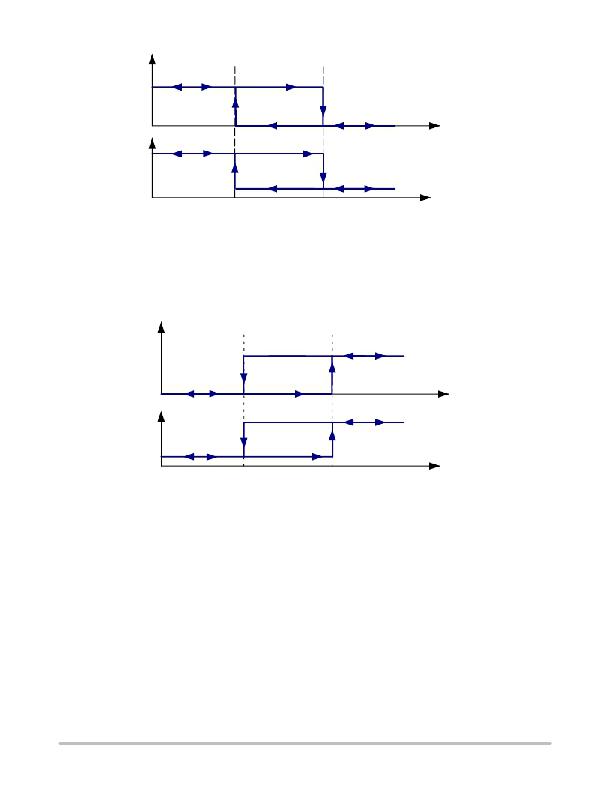
�NCP1910�
�State�
�ON�
�OFF�
�I� CC�
�TBD�
�<� 600� m� A�
�On/off� pin�
�V� on�
�V� off�
�On/off� pin�
�Figure� 62.� Remote� on/off� (on/off� Pin)�
�V� CC� Under� ?� Voltage� LockOut� (UVLO)�
�The� device� incorporates� an� Under� ?� Voltage� Lockout� block�
�to� prevent� the� circuit� from� operating� when� V� CC� is� too� low� in�
�order� to� ensure� a� proper� operation.� An� UVLO� comparator�
�monitors� V� CC� pin� voltage� to� allow� the� NCP1910� to� operate�
�when� V� CC� exceeds� V� CC(on)� .� The� comparator� incorporates�
�some� hysteresis� (V� CC(Hys)� )� to� prevent� erratic� operation� as�
�the� V� CC� crosses� the� threshold.� When� V� CC� goes� below� the�
�UVLO� comparator� lower� threshold� (V� CC(min)� ),� the� circuit�
�turns� off.� It� is� illustrated� in� Figure� 63.� After� startup,� the�
�operating� range� is� between� 9� V� and� 20� V.�
�State�
�ON�
�OFF�
�TBD�
�V� CC�
�I� CC�
�<� 100� m� A�
�V� CC(min)�
�V� CC(on)�
�V� CC�
�Figure� 63.� V� CC� Under� ?� Voltage� LockOut� (UVLO)�
�Bias� the� Controller�
�It� is� recommended� to� add� a� typical� 1� nF� to� 100� nF�
�decoupling� capacitor� next� to� the� V� CC� pin� for� proper�
�operation.� The� hysteresis� between� V� CC(on)� and� V� CC(min)� is�
�small� because� the� NCP1910� is� supposed� to� be� biased� by�
�external� power� source.� Therefore� it� is� recommended� to�
�make� a� low� ?� voltage� source� to� bias� NCP1910,� e.g.� the�
�standby� power� supply.�
�Thermal� Shutdown�
�An� internal� thermal� circuitry� disables� the� circuit� gate� drive�
�and� then� keeps� the� power� switch� off� when� the� junction�
�temperature� exceeds� TSD� level.� The� output� stage� is� then�
�enabled� once� the� temperature� drops� below� typically� 110� °� C�
�(i.e.� TSD� ?� TSD� hyste� ).� The� thermal� shutdown� is� provided� to�
�prevent� possible� device� failures� that� could� result� from� an�
�accidental� over� ?� heating.�
�5� V� Reference�
�The� V� REF� pin� provides� an� accurate� (� ±� 2%� typically)� 5� V�
�reference� voltage.� The� Power� ?� Good� and� Brown� ?� Out� of�
�LLC� converter,� and� the� frequency� foldback� level� (fold� pin)�
�of� PFC� can� hence� can� get� an� accurate� reference� voltage� by�
�resistor� dividers.�
�http://onsemi.com�
�35�
�相关PDF资料 |
PDF描述 |
|---|---|
| NCP3418BMNR2G | IC MOSFET DRIVER DUAL 12V 10-DFN |
| NCP3418DR2 | IC MOSFET DRIVER DUAL 12V 8-SOIC |
| NCP3420DR2G | IC MOSFET DRIVER DUAL 12V 8-SOIC |
| NCP3488DR2G | IC MOSFET DRVR DUAL 12V 8-SOIC |
| NCP5007SNT1 | IC LED DRIVR WHT COMPACT 5TSOP |
相关代理商/技术参数 |
参数描述 |
|---|---|
| NCP1927DR2G | 功能描述:功率因数校正 IC PFC AND FLYBACK CONTROLER RoHS:否 制造商:Fairchild Semiconductor 开关频率:300 KHz 最大功率耗散: 最大工作温度:+ 125 C 安装风格:SMD/SMT 封装 / 箱体:SOIC-8 封装:Reel |
| NCP1937A1DR2G | 制造商:ON Semiconductor 功能描述:COMBO PFC & QUAZI FLYBACK - Tape and Reel 制造商:ON Semiconductor 功能描述:REEL / COMBO PFC & QUAZI FLYBACK |
| NCP1937B1DR2G | 制造商:ON Semiconductor 功能描述:COMBO PFC & QUAZI FLYBACK - Tape and Reel |
| NCP1937BADAPGEVB | 制造商:ON Semiconductor 功能描述:ADPTR 90W PFC+QR<10MW - Bulk 制造商:ON Semiconductor 功能描述:BOARD EVAL FOR NCP1937 制造商:ON Semiconductor 功能描述:Power Management IC Development Tools 90 W Adapter PFC+QR 10 MW Eval Brd |
| NCP21WB333 | 制造商:MURATA 制造商全称:Murata Manufacturing Co., Ltd. 功能描述:for Surface Mounting Application |
发布紧急采购,3分钟左右您将得到回复。