- 您现在的位置:买卖IC网 > Datasheet目录345 > NCP1910GEVB (ON Semiconductor)BOARD DEMO NCP1910DEMO-B-TLS Datasheet资料下载
参数资料
| 型号: | NCP1910GEVB |
| 厂商: | ON Semiconductor |
| 文件页数: | 22/37页 |
| 文件大小: | 0K |
| 描述: | BOARD DEMO NCP1910DEMO-B-TLS |
| 设计资源: | NCP1910 Schematic NCP1910GEVB BOM |
| 标准包装: | 1 |
| 主要目的: | DC/DC,步降 |
| 输出及类型: | 1,非隔离 |
| 输出电压: | 最低可调至 0.8V |
| 电流 - 输出: | 3A |
| 输入电压: | 3 ~ 5.5 V |
| 稳压器拓扑结构: | 降压 |
| 频率 - 开关: | 1MHz |
| 板类型: | 完全填充 |
| 已供物品: | 板 |
| 已用 IC / 零件: | NCP1910 |
| 其它名称: | NCP1910GEVBOS |
第1页第2页第3页第4页第5页第6页第7页第8页第9页第10页第11页第12页第13页第14页第15页第16页第17页第18页第19页第20页第21页当前第22页第23页第24页第25页第26页第27页第28页第29页第30页第31页第32页第33页第34页第35页第36页第37页
�� �
�
�NCP1910�
�V� M� +�
�R� M� I� CS� V� LBO� 2�
�4� V� CTRL� *� V� CTRL� min�
�PFC� Duty�
�V� M�
�11�
�I� M�
�R� M�
�C� M�
�Modulation�
�Figure� 45.� The� Multiplier� Voltage� Pin� Configuration�
�The� multiplier� voltage� V� M� is� generated� according� to�
�Equation� 8.�
�?�
�V� CTRL� is� the� control� voltage� signal,� the� output�
�voltage� of� Operational� Trans� ?� conductance� Amplifier�
�R� M� I� CS� V� LBO�
�2�
�V� M� +� (eq.� 8)�
�4� V� CTRL� *� V� CTRL(min)�
�Where:�
�?� R� M� is� the� external� multiplier� resistor� connected� to�
�V� M� pin,� which� is� constant.�
�?� V� LBO� is� the� input� voltage� signal� appearing� on� the�
�LBO� pin,� which� is� proportional� to� the� rms� input�
�voltage,�
�?� I� CS� is� the� sense� current� proportional� to� the� inductor�
�current� I� L� as� described� in� Equation� 13.�
�Line� Brown� ?� Out� Protection�
�V� in�
�Ac� line�
�(OTA),� as� described� in� Equation� 17.�
�?� V� CTRL(min)� is� not� only� the� minimum� operating�
�voltage� of� V� CTRL� but� also� the� offset� voltage� for� the�
�PFC� current� modulation.�
�R� M� directly� limits� the� maximum� input� power� capability.�
�Also,� due� to� the� V� in2� feed� ?� forward� feature,� where� the� V� LBO�
�is� squared,� the� transfer� function� and� the� power� delivery� is�
�independent� from� the� ac� line� level.� The� relationship� between�
�V� CTRL� and� power� delivery� will� be� depicted� later� on.�
�EMI�
�Filter�
�C� in�
�R� LBOU�
�LBO�
�V� LBOT�
�LBO� comp.�
�V� LBOcomp�
�PFC_BO�
�R� SENSE�
�C� LBO�
�R� LBOL�
�S�
�L� BO� Q�
�t� LBO(blank)�
�t� LBO(window)�
�Vdd�
�V� LBO(clamp)�
�R�
�reset�
�reset�
�reset�
�I� LBOH�
�Figure� 46.� The� Line� Brown� ?� Out� Configuration�
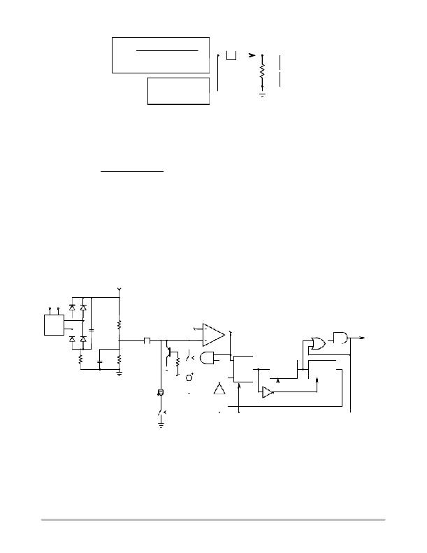
�As� shown� in� Figure� 46,� the� Line� Brown� ?� Out� pin�
�(represented� LBO� pin)� as� receives� a� portion� of� the� input�
�voltage� (V� in� ).� As� V� in� is� a� rectified� sinusoid,� a� capacitor� must�
�integrate� the� ac� line� ripple� so� that� a� voltage� proportional� to�
�the� average� value� of� V� in� is� applied� to� the� brown� ?� out� pin.�
�The� main� function� of� the� LBO� block� is� to� detect� too� low�
�input� voltage� conditions.� A� 7� m� A� current� source� lowers� the�
�LBO� pin� voltage� when� a� brown� ?� out� condition� is� detected.�
�This� is� for� hysteresis� purpose� as� required� by� this� function.�
�In� nominal� operation,� the� voltage� applied� to� LBO� pin� must�
�be� above� the� internal� reference� voltage,� V� LBOT� (1� V�
�typically).� In� this� case,� the� output� of� the� LBO� comparator�
�V� LBOcomp� is� low.�
�http://onsemi.com�
�22�
�相关PDF资料 |
PDF描述 |
|---|---|
| NCP3418BMNR2G | IC MOSFET DRIVER DUAL 12V 10-DFN |
| NCP3418DR2 | IC MOSFET DRIVER DUAL 12V 8-SOIC |
| NCP3420DR2G | IC MOSFET DRIVER DUAL 12V 8-SOIC |
| NCP3488DR2G | IC MOSFET DRVR DUAL 12V 8-SOIC |
| NCP5007SNT1 | IC LED DRIVR WHT COMPACT 5TSOP |
相关代理商/技术参数 |
参数描述 |
|---|---|
| NCP1927DR2G | 功能描述:功率因数校正 IC PFC AND FLYBACK CONTROLER RoHS:否 制造商:Fairchild Semiconductor 开关频率:300 KHz 最大功率耗散: 最大工作温度:+ 125 C 安装风格:SMD/SMT 封装 / 箱体:SOIC-8 封装:Reel |
| NCP1937A1DR2G | 制造商:ON Semiconductor 功能描述:COMBO PFC & QUAZI FLYBACK - Tape and Reel 制造商:ON Semiconductor 功能描述:REEL / COMBO PFC & QUAZI FLYBACK |
| NCP1937B1DR2G | 制造商:ON Semiconductor 功能描述:COMBO PFC & QUAZI FLYBACK - Tape and Reel |
| NCP1937BADAPGEVB | 制造商:ON Semiconductor 功能描述:ADPTR 90W PFC+QR<10MW - Bulk 制造商:ON Semiconductor 功能描述:BOARD EVAL FOR NCP1937 制造商:ON Semiconductor 功能描述:Power Management IC Development Tools 90 W Adapter PFC+QR 10 MW Eval Brd |
| NCP21WB333 | 制造商:MURATA 制造商全称:Murata Manufacturing Co., Ltd. 功能描述:for Surface Mounting Application |
发布紧急采购,3分钟左右您将得到回复。