- 您现在的位置:买卖IC网 > Datasheet目录345 > NCP1910GEVB (ON Semiconductor)BOARD DEMO NCP1910DEMO-B-TLS Datasheet资料下载
参数资料
| 型号: | NCP1910GEVB |
| 厂商: | ON Semiconductor |
| 文件页数: | 30/37页 |
| 文件大小: | 0K |
| 描述: | BOARD DEMO NCP1910DEMO-B-TLS |
| 设计资源: | NCP1910 Schematic NCP1910GEVB BOM |
| 标准包装: | 1 |
| 主要目的: | DC/DC,步降 |
| 输出及类型: | 1,非隔离 |
| 输出电压: | 最低可调至 0.8V |
| 电流 - 输出: | 3A |
| 输入电压: | 3 ~ 5.5 V |
| 稳压器拓扑结构: | 降压 |
| 频率 - 开关: | 1MHz |
| 板类型: | 完全填充 |
| 已供物品: | 板 |
| 已用 IC / 零件: | NCP1910 |
| 其它名称: | NCP1910GEVBOS |
第1页第2页第3页第4页第5页第6页第7页第8页第9页第10页第11页第12页第13页第14页第15页第16页第17页第18页第19页第20页第21页第22页第23页第24页第25页第26页第27页第28页第29页当前第30页第31页第32页第33页第34页第35页第36页第37页
�� �
�
�NCP1910�
�PFC� Abnormal�
�The� PFC� abnormal� is� detected� by� sensing� V� CTRL� level.�
�When� V� CTRL� stays� at� V� CTRL(max)� ,� or� lower� than� V� CTRL(min)�
�–� 0.1� V,� for� more� than� t� PFCabnormal� ,� PFC� turns� off� first.� After�
�t� DEL2� ,� LLC� shuts� down.� It� is� latches� off� protection.�
�The� main� purpose� of� this� feature� is� to� avoid� LLC� from�
�operating� without� correct� operation� of� PFC� stage.�
�LLC� Section�
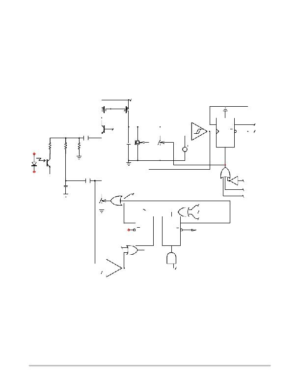
�Current� Controlled� Oscillator� (CCO)�
�The� current� controlled� oscillator� features� a� high� ?� speed�
�circuitry� allowing� operation� from� 50� kHz� up� to� 1� MHz.�
�VDD�
�However,� as� a� D� ?� flip� ?� flop� that� creates� division� ?� by� ?� two�
�internally� provides� two� outputs� (A� and� B� in� Figure� 57),� the�
�final� effective� signal� on� LLC� driver� outputs� (ML� and� MU)�
�switches� between� 25� kHz� and� 500� kHz.� The� CCO� is�
�configured� in� such� a� way� that� if� the� current� that� flows� out�
�from� the� R� t� pin� increases,� the� switching� frequency� also� goes�
�up.�
�R� max�
�R� SS�
�R� t�
�R� min�
�V� Rt�
�C� t�
�I� DT�
�+�
�-�
�V� Ctmax�
�S�
�D�
�Clk�
�R�
�Q�
�Q�
�B�
�A�
�for� MU�
�for� ML�
�Feedback�
�opto-coupler�
�C� SS�
�SS�
�Grand� Reset�
�CS/FF� >� V� CS1�
�LLC_BO�
�t� DEL2� elapsed�
�LLCenable�
�Grand� Reset�
�Latch�
�Q�
�Q�
�S�
�S�
�Q�
�Q�
�Grand� Reset�
�Disable� LLC� ML� and� MU�
�Grand� Reset�
�V� SS_RST�
�R�
�R�
�LLC_PG�
�Figure� 57.� The� Current� Controlled� Oscillator� Architecture� and� Configuration�
�The� internal� timing� capacitor� C� t� is� charged� by� current�
�which� is� proportional� to� the� current� flowing� out� from� the�
�R� t� pin.� The� discharging� current� i� DT� is� applied� when� voltage�
�on� this� capacitor� reaches� V� Ctmax� .� The� output� drivers� are�
�disabled� during� discharge� period� so� the� dead� time� length� is�
�given� by� the� discharge� current� sink� capability.� Discharge�
�sink� is� disabled� when� voltage� on� the� timing� capacitor�
�reaches� zero� and� charging� cycle� starts� again.� C� t� is� grounded�
�to� disable� the� oscillator� when� either� of� “turn� ?� off� LLC”�
�For� the� resonant� applications,� it� is� necessary� to� adjust�
�minimum� operating� frequency� with� high� accuracy.� The�
�designer� also� needs� to� limit� maximum� operating� and� startup�
�frequency.� All� these� parameters� can� be� adjusted� by� using�
�external� components� connected� to� the� R� t� pin� as� shown� in�
�Figure� 57.�
�The� following� approximate� relationships� hold� for� the�
�minimum,� maximum� and� startup� frequency� respectively:�
�signals� arrives.�
�http://onsemi.com�
�30�
�相关PDF资料 |
PDF描述 |
|---|---|
| NCP3418BMNR2G | IC MOSFET DRIVER DUAL 12V 10-DFN |
| NCP3418DR2 | IC MOSFET DRIVER DUAL 12V 8-SOIC |
| NCP3420DR2G | IC MOSFET DRIVER DUAL 12V 8-SOIC |
| NCP3488DR2G | IC MOSFET DRVR DUAL 12V 8-SOIC |
| NCP5007SNT1 | IC LED DRIVR WHT COMPACT 5TSOP |
相关代理商/技术参数 |
参数描述 |
|---|---|
| NCP1927DR2G | 功能描述:功率因数校正 IC PFC AND FLYBACK CONTROLER RoHS:否 制造商:Fairchild Semiconductor 开关频率:300 KHz 最大功率耗散: 最大工作温度:+ 125 C 安装风格:SMD/SMT 封装 / 箱体:SOIC-8 封装:Reel |
| NCP1937A1DR2G | 制造商:ON Semiconductor 功能描述:COMBO PFC & QUAZI FLYBACK - Tape and Reel 制造商:ON Semiconductor 功能描述:REEL / COMBO PFC & QUAZI FLYBACK |
| NCP1937B1DR2G | 制造商:ON Semiconductor 功能描述:COMBO PFC & QUAZI FLYBACK - Tape and Reel |
| NCP1937BADAPGEVB | 制造商:ON Semiconductor 功能描述:ADPTR 90W PFC+QR<10MW - Bulk 制造商:ON Semiconductor 功能描述:BOARD EVAL FOR NCP1937 制造商:ON Semiconductor 功能描述:Power Management IC Development Tools 90 W Adapter PFC+QR 10 MW Eval Brd |
| NCP21WB333 | 制造商:MURATA 制造商全称:Murata Manufacturing Co., Ltd. 功能描述:for Surface Mounting Application |
发布紧急采购,3分钟左右您将得到回复。