- 您现在的位置:买卖IC网 > PDF目录20679 > NCV8855BMNR2G (ON Semiconductor)IC REG QD BUCK/LINEAR 40QFN PDF资料下载
参数资料
| 型号: | NCV8855BMNR2G |
| 厂商: | ON Semiconductor |
| 文件页数: | 15/24页 |
| 文件大小: | 0K |
| 描述: | IC REG QD BUCK/LINEAR 40QFN |
| 标准包装: | 1 |
| 拓扑: | 降压(降压)(2),线性(LDO)(2) |
| 功能: | 汽车无线电设备和仪表板电源 |
| 输出数: | 4 |
| 频率 - 开关: | 170kHz |
| 电压/电流 - 输出 1: | 控制器 |
| 电压/电流 - 输出 2: | 可调式,2.5A |
| 电压/电流 - 输出 3: | 控制器 |
| 带 LED 驱动器: | 无 |
| 带监控器: | 无 |
| 带序列发生器: | 是 |
| 电源电压: | 9 V ~ 18 V |
| 工作温度: | -40°C ~ 105°C |
| 安装类型: | 表面贴装 |
| 封装/外壳: | 40-VFQFN 裸露焊盘 |
| 供应商设备封装: | 40-QFN(6x6) |
| 包装: | 标准包装 |
| 其它名称: | NCV8855BMNR2GOSDKR |
�� �
�
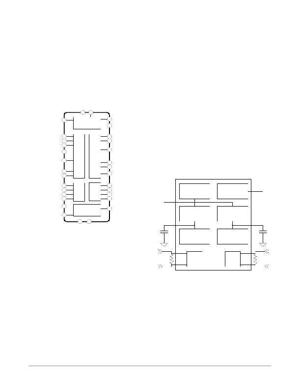
�NCV8855�
�THEORY� OF� OPERATION�
�Device� Description�
�The� NCV8855� is� a� multiple� output� controller� /� regulator�
�IC� with� an� integrated� high� ?� side� load� switch.� The� NCV8855�
�will� address� automotive� radio� system� and� instrument� cluster�
�power� supply� requirements.� In� addition� to� the� high� ?� side�
�load� switch,� the� NCV8855� comprise� a� switch� ?� mode� power�
�supply� (SMPS)� buck� controller,� a� 2� A� SMPS� buck� regulator,�
�and� two� low� dropout� linear� regulator� controllers� (LDO).� The�
�NCV8855� in� combination� with� the� ultra� ?� low� Iq� NCV861x�
�IC� forms� an� eight� output� automotive� radio� or� instrument�
�cluster� power� solution.�
�DRV_VPP� 5V_IC�
�Linear� Regulator� Enable� (LDO_EN)�
�The� low� ?� dropout� linear� regulators� (LDOs)� have� a�
�dedicated� enable� pin.� This� pin� controls� the� startup� and�
�shutdown� of� the� LDOs.� The� SYS_EN� pin� must� be� logic� high�
�for� this� pin� to� function.� It� is� possible� to� drive� this� pin� high�
�coincidentally� with� SYS_EN,� but� the� LDO� outputs� will� not�
�startup� until� DRV_VPP� and� 5V_IC� have� increased� above� its�
�UVLO� thresholds.�
�High� ?� Side� Switch� Enable� (HS_EN)�
�The� high� ?� side� switch� enable� controls� only� the� high� ?� side�
�switch.� Similar� to� LDO_EN,� the� SYS_EN� pin� must� be� logic�
�high� for� this� pin� to� function.� The� voltage� level� on� all� enable�
�22�
�35�
�pins� have� been� designed� to� work� with� 3.3� V� or� 5� V� logic.�
�4� SYNC/�
�SYS_EN� 5�
�BST1� 25�
�GH1� 24�
�SN1� 23�
�GL1� 21�
�OCSET� 27�
�SW_FB1� 29�
�COMP1� 30�
�MAIN�
�6� LDO_EN�
�8� HOT_FLG�
�11� BST2�
�10� VIN_SW�
�9� SN2�
�3� SW_FB2�
�2� COMP2�
�ROSC�
�IC� Power� (VIN,� VIN_SW,� DRV_VPP,� 5V_IC)�
�There� are� many� input� voltage� rails� for� the� NCV8855.� The�
�main� power� supply� input� for� the� IC� is� VIN.� The� DRV_VPP,�
�5V_IC� and� the� high� ?� side� switch� drain� are� all� driven� from�
�V� IN� .� The� DRV_VPP� voltage� rail� is� the� power� rail� for� SMPS1�
�&� SMPS2’s� gate� driver� circuits.� The� 5V_IC� voltage� rail� is�
�the� main� supply� for� the� IC.� The� VIN_SW� rail� is� the� supply�
�rail� for� SMPS2’s� internal� upper� MOSFET.� VIN_SW� is�
�directly� tied� to� the� drain� of� the� N� ?� channel� MOSFET.�
�ISNS1+� 40�
�ISNS1� ?� 39�
�LR_G1� 1�
�LR_FB1� 38�
�31�
�32�
�33�
�34�
�ISNS2+�
�ISNS2� ?�
�LR_G2�
�LR_FB2�
�VIN�
�High� ?� Side�
�Switch�
�SMPS2�
�Internal� upper�
�MOSFET�
�VIN_SW�
�VIN� 26�
�HS_S� 28�
�HIGH� ?� SIDE�
�SWITCH�
�37� 20�
�7� HS_EN�
�DRV_VPP�
�DRV_VPP�
�internal�
�regulator�
�5V_IC� internal�
�regulator�
�5V_IC�
�AGND� PGND�
�Figure� 17.�
�The� NCV8855� has� an� internally� set� switching� frequency�
�of� 170� kHz� and� provides� an� SYNC� pin� for� external�
�frequency� synchronization.� The� NCV8855� is� designed� to�
�operate� within� the� range� of� 9� V� to� 18� V.� The� switch� ?� mode�
�power� supplies� are� voltage� ?� mode� controlled� and� the� LDO�
�ISNS1+�
�ISNS1� ?�
�SMPS1� &� 2�
�Gate� Drivers�
�LDO1�
�Main� IC�
�LDO2�
�I� SNS2+�
�ISNS2� ?�
�controllers� drive� P� ?� channel� MOSFETs� as� pass� devices.�
�System� Enable� (SYS_EN)�
�The� system� enable� (SYS_EN)� pin� is� used� to� start� device�
�operation� or� place� it� in� low� quiescent� shutdown.� Driving� this�
�pin� high� will� allow� the� two� main� internal� voltage� rails�
�(DRV_VPP� and� 5V_IC)� to� power� up.� These� voltage� rails�
�require� external� bypassing� and� have� independent� UVLO� trip�
�points.� Both� rails� must� be� operational� in� order� for� the� IC� to�
�function.� After� exceeding� its� UVLO� threshold,� the� IC� will�
�power� up� the� switch� ?� mode� power� supplies� with� a� soft� ?� start.�
�Conversely,� a� logic� ?� low� on� the� pin� will� power� down� the�
�DRV_VPP� and� 5V_IC� rails� and� place� the� IC� in� an� ultra� ?� low�
�Figure� 18.�
�Two� additional� inputs� rails� are� ISNS1+� and� ISNS2+.�
�These� inputs� not� only� serve� as� the� positive� reference� for� the�
�current� sense� circuit,� but� also� serve� as� the� supply� rail� for� the�
�LDO� error� amplifier.�
�Startup� and� Shutdown� Behavior�
�The� startup� sequence� primary� depends� on� the� system�
�configuration.� However,� in� every� case,� enable� SYS_EN�
�first.� The� SYNC� pin� must� not� be� held� at� logic� high� before�
�SYS_EN� is� enabled.� Below� shows� typical� startup� and�
�current� shutdown� state.�
�http://onsemi.com�
�15�
�相关PDF资料 |
PDF描述 |
|---|---|
| VE-JNF-CX-F2 | CONVERTER MOD DC/DC 72V 75W |
| TH3C106K016E1400 | CAP TANT 10UF 16V 10% 2312 |
| FMC20DRXH | CONN EDGECARD 40POS DIP .100 SLD |
| ISL6207HBZ-T | IC MOSFET DRVR SYNC BUCK 8-SOIC |
| VE-2N0-EW-B1 | CONVERTER MOD DC/DC 5V 100W |
相关代理商/技术参数 |
参数描述 |
|---|---|
| NCV8855BMNR2GEVB | 功能描述:电源管理IC开发工具 SMPS ASIC RoHS:否 制造商:Maxim Integrated 产品:Evaluation Kits 类型:Battery Management 工具用于评估:MAX17710GB 输入电压: 输出电压:1.8 V |
| NCV8870 | 制造商:ONSEMI 制造商全称:ON Semiconductor 功能描述:Automotive Grade Non-Synchronous Boost Controller |
| NCV887000 | 制造商:ONSEMI 制造商全称:ON Semiconductor 功能描述:Automotive Grade Non-Synchronous Boost Controller |
| NCV887000D1R2G | 功能描述:低压差稳压器 - LDO Auto Grade Non-Sync Boost Controller RoHS:否 制造商:Texas Instruments 最大输入电压:36 V 输出电压:1.4 V to 20.5 V 回动电压(最大值):307 mV 输出电流:1 A 负载调节:0.3 % 输出端数量: 输出类型:Fixed 最大工作温度:+ 125 C 安装风格:SMD/SMT 封装 / 箱体:VQFN-20 |
| NCV887001 | 制造商:ONSEMI 制造商全称:ON Semiconductor 功能描述:Automotive Grade Non-Synchronous Boost Controller |
发布紧急采购,3分钟左右您将得到回复。