- 您现在的位置:买卖IC网 > PDF目录20679 > NCV8855BMNR2G (ON Semiconductor)IC REG QD BUCK/LINEAR 40QFN PDF资料下载
参数资料
| 型号: | NCV8855BMNR2G |
| 厂商: | ON Semiconductor |
| 文件页数: | 21/24页 |
| 文件大小: | 0K |
| 描述: | IC REG QD BUCK/LINEAR 40QFN |
| 标准包装: | 1 |
| 拓扑: | 降压(降压)(2),线性(LDO)(2) |
| 功能: | 汽车无线电设备和仪表板电源 |
| 输出数: | 4 |
| 频率 - 开关: | 170kHz |
| 电压/电流 - 输出 1: | 控制器 |
| 电压/电流 - 输出 2: | 可调式,2.5A |
| 电压/电流 - 输出 3: | 控制器 |
| 带 LED 驱动器: | 无 |
| 带监控器: | 无 |
| 带序列发生器: | 是 |
| 电源电压: | 9 V ~ 18 V |
| 工作温度: | -40°C ~ 105°C |
| 安装类型: | 表面贴装 |
| 封装/外壳: | 40-VFQFN 裸露焊盘 |
| 供应商设备封装: | 40-QFN(6x6) |
| 包装: | 标准包装 |
| 其它名称: | NCV8855BMNR2GOSDKR |
�� �
�
�NCV8855�
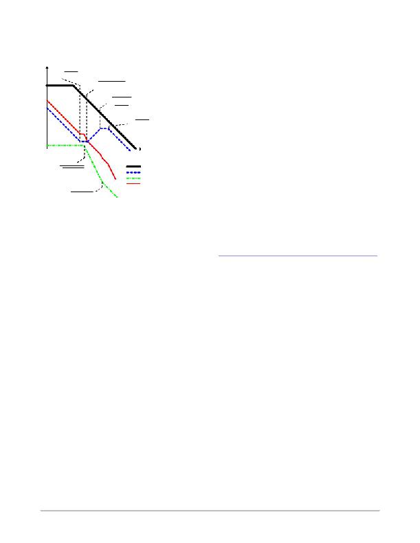
�control� loop� has� a� gain� crossing� with� ?� 20� dB/decade� slope�
�and� a� phase� margin� greater� than� 45� °� .�
�gain� =� 0� dB� or� a� gain� of� 1.� In� the� plot� above,� the� UGB� is� the�
�point� where� the� red� line� crosses� the� W� axis.� Goal� 2� is� to� have�
�the� closed� loop� gain� cross� 0� dB� with� a� ?� 20� dB/decade� slope�
�dB�
�w� Z1� +�
�1�
�R� 2� @� C� 2�
�w� Z2� +�
�1�
�R� 1� )� R� 3� @� C� 3�
�1�
�w� P1� +�
�C� 1� @� C� 2�
�C� 1� )� C� 2�
�w� P2� +�
�1�
�R� 3� @� C� 3�
�also� known� as� a� ?� 1� slope.� Goal� 3� is� to� achieve� over� 45� °� of�
�phase� margin� when� the� gain� crosses� 0� dB.�
�These� are� just� goals.� Sometimes� the� crossover� frequency�
�is� reduced� below� 1/10� FSW� in� order� to� meet� goal� 3.�
�Conversely,� some� designs� will� push� the� crossover� frequency�
�as� high� as� it� can� (as� long� as� it� is� below� 1/2� FSW)� with� a�
�reduce� phase� margin� of� 30� °� in� order� to� get� a� faster� transient�
�response.� The� only� two� absolutes� are� that� the� crossover�
�frequency� cannot� exceed� 1/2� FSW� and� the� phase� margin� has�
�w�
�to� be� greater� than� 0� °� at� crossover.� However,� a� SMPS�
�operating� towards� these� absolutes� will� experience� sever�
�ringing� before� it� dampens� out.�
�1�
�w� LC� +�
�L� OUT� @� C� OUT�
�1�
�w� ESR� +�
�ESR� @� C� OUT�
�Error� Amplifier�
�Compensation� Network�
�Modulator� Gain�
�Closed� Loop� Gain�
�To� achieve� the� above� goals,� the� following� guidelines�
�should� be� adopted.�
�?� Place� wZ1� at� half� the� resonance� of� wLC�
�?� Place� wZ2� at� or� around� wLC�
�?� Place� wP1� at� wESR�
�Figure� 27.�
�To� reiterate,� there� are� 3� primary� goals� to� compensating.�
�Goal� 1� is� to� have� a� high� a� unity� gain� bandwidth� (UGB)� that�
�is� greater� than� 1/10� the� switching� frequency,� but� less� than� 1/2�
�the� switching� frequency.� UGB� is� also� known� as� the�
�crossover� frequency.� This� is� the� point� where� the� closed� loop�
�?� Place� wP2� at� half� the� switching� frequency�
�Performing� these� calculations� will� take� some� amount� of�
�iterations� and� bench� testing� to� verify� results.� However,�
�ON� Semiconductor� has� developed� a� tool� to� speed� up� the�
�design� process� tremendously� with� great� ease� and� accuracy.�
�This� tool� can� be� downloaded� by� following� the� below� link.�
�http://www.onsemi.com/pub/Collateral/COMPCALC.ZIP�
�http://onsemi.com�
�21�
�相关PDF资料 |
PDF描述 |
|---|---|
| VE-JNF-CX-F2 | CONVERTER MOD DC/DC 72V 75W |
| TH3C106K016E1400 | CAP TANT 10UF 16V 10% 2312 |
| FMC20DRXH | CONN EDGECARD 40POS DIP .100 SLD |
| ISL6207HBZ-T | IC MOSFET DRVR SYNC BUCK 8-SOIC |
| VE-2N0-EW-B1 | CONVERTER MOD DC/DC 5V 100W |
相关代理商/技术参数 |
参数描述 |
|---|---|
| NCV8855BMNR2GEVB | 功能描述:电源管理IC开发工具 SMPS ASIC RoHS:否 制造商:Maxim Integrated 产品:Evaluation Kits 类型:Battery Management 工具用于评估:MAX17710GB 输入电压: 输出电压:1.8 V |
| NCV8870 | 制造商:ONSEMI 制造商全称:ON Semiconductor 功能描述:Automotive Grade Non-Synchronous Boost Controller |
| NCV887000 | 制造商:ONSEMI 制造商全称:ON Semiconductor 功能描述:Automotive Grade Non-Synchronous Boost Controller |
| NCV887000D1R2G | 功能描述:低压差稳压器 - LDO Auto Grade Non-Sync Boost Controller RoHS:否 制造商:Texas Instruments 最大输入电压:36 V 输出电压:1.4 V to 20.5 V 回动电压(最大值):307 mV 输出电流:1 A 负载调节:0.3 % 输出端数量: 输出类型:Fixed 最大工作温度:+ 125 C 安装风格:SMD/SMT 封装 / 箱体:VQFN-20 |
| NCV887001 | 制造商:ONSEMI 制造商全称:ON Semiconductor 功能描述:Automotive Grade Non-Synchronous Boost Controller |
发布紧急采购,3分钟左右您将得到回复。