- 您现在的位置:买卖IC网 > PDF目录20679 > NCV8855BMNR2G (ON Semiconductor)IC REG QD BUCK/LINEAR 40QFN PDF资料下载
参数资料
| 型号: | NCV8855BMNR2G |
| 厂商: | ON Semiconductor |
| 文件页数: | 16/24页 |
| 文件大小: | 0K |
| 描述: | IC REG QD BUCK/LINEAR 40QFN |
| 标准包装: | 1 |
| 拓扑: | 降压(降压)(2),线性(LDO)(2) |
| 功能: | 汽车无线电设备和仪表板电源 |
| 输出数: | 4 |
| 频率 - 开关: | 170kHz |
| 电压/电流 - 输出 1: | 控制器 |
| 电压/电流 - 输出 2: | 可调式,2.5A |
| 电压/电流 - 输出 3: | 控制器 |
| 带 LED 驱动器: | 无 |
| 带监控器: | 无 |
| 带序列发生器: | 是 |
| 电源电压: | 9 V ~ 18 V |
| 工作温度: | -40°C ~ 105°C |
| 安装类型: | 表面贴装 |
| 封装/外壳: | 40-VFQFN 裸露焊盘 |
| 供应商设备封装: | 40-QFN(6x6) |
| 包装: | 标准包装 |
| 其它名称: | NCV8855BMNR2GOSDKR |
�� �
�
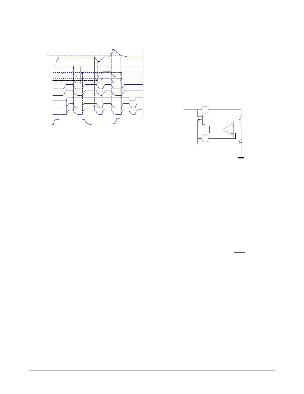
�NCV8855�
�shutdown� behavior� when� VOUT3� is� derived� from� VOUT1�
�(as� shown� in� Figure� 1).�
�Startup� and� Shutdown� Behavior�
�18.5� V�
�17.9� V�
�re� ?� start� the� high� ?� side� switch� in� the� case� of� a� T� MON_HSS� TSD�
�event.�
�If� thermal� monitor� 2� (T� MON_SW� )� exceeds� it� TSD� point,� the�
�entire� chip� (regardless� of� the� state� of� T� MON_HSS� )� will� latch�
�off,� and� a� SYS_EN� toggle� will� be� required� to� restart.�
�VIN�
�SYS_EN�
�8V_IC�
�5V_IC�
�VOUT1�
�VOUT2�
�LDO_EN�
�VOUT3�
�VOUT4�
�>2.2� V�
�<0.8� V�
�4.35� V�
�4.2� V�
�4.35� V�
�4.2� V�
�>2.2� V�
�<0.8� V�
�Overcurrent� Protection� (SMPS1)�
�Overcurrent� protection� for� SMPS1� is� implemented� via�
�V� DS(on)� sensing� of� the� upper� MOSFET.� At� the� beginning� of�
�each� switching� cycle,� after� a� short� blanking� time,� the� voltage�
�is� sampled� across� the� upper� MOSFET� and� compared� to� the�
�threshold� set� by� R� OCSET� .�
�OCSET�
�27�
�Natural� Startup�
�Natural� Decay�
�Controlled� Soft� ?� Star�
�External� upper�
�MOSFET�
�ROCSET�
�Figure� 19.�
�ILIMIT�
�In� addition� to� the� enable� pins,� the� IC� features� an� automatic�
�shutdown� during� a� high� battery� condition.� When� VIN�
�exceeds� 18.5� V� (typ)� the� IC� will� shutdown� all� outputs.� When�
�23�
�SN1�
�50� A�
�I� LIMIT� +�
�I� pk� ?� pk�
�I� LIMIT� w� IOUT1� MAX� )�
�V� IN� falls� below� 17.9� V� (typ),� the� IC� will� go� through� a� typical�
�start� up� and� resume� normal� operation.�
�Out� ?� of� ?� Phase� Synchronization�
�By� default,� the� turn� ?� on� of� SMPS2� is� delayed� by� half� the�
�switching� cycle,� which� corresponds� to� 180� °� phase� delay.�
�Advantages� of� out� ?� of� ?� phase� synchronization� are� many.�
�Interleaving� the� current� pulses� at� the� input� reduces� the� input�
�RMS� current.� This� reduction� minimizes� the� input� filter�
�requirement,� allowing� the� use� of� smaller� components,� hence�
�a� more� cost� effective� solution.� In� addition,� since� peak� current�
�is� reduced,� emitted� EMI� is� also� reduced.�
�Synchronizing� (SYNC)�
�Synchronizing� the� NCV8855� to� an� external� frequency� is�
�achieved� by� providing� a� 10� to� 90%� duty� cycle� clock� to� the�
�SNYC� pin.� The� rising� edge� of� the� clock� signal� will�
�immediately� reset� the� internal� RAMP� of� SMPS2� and� begin�
�a� new� pulse� for� SMPS2.� Conversely,� the� falling� edge� of� the�
�clock� signal� will� immediately� reset� the� internal� RAMP� of�
�SMPS1� and� begin� a� new� pulse� for� SMPS1.� The� first� rising�
�edge� of� the� external� clock� signal� may� cause� a� momentary�
�phase� diversion� between� SMPS1� and� SMPS2,� but� will� lock�
�into� desired� phase� on� the� subsequent� falling� edge.� During�
�start� up,� the� SYNC� pin� must� not� be� held� at� a� logic� high.�
�Thermal� Warning� (HOT_FLG)� and� Thermal� Shutdown�
�There� are� two� thermal� sensors� in� the� NCV8855� devices.�
�If� any� of� these� two� exceeds� the� warning� threshold,� the�
�HOT_FLG� will� assert� low.� In� addition,� if� thermal� monitor� 1�
�(T� MON_HSS� )� exceeds� the� warning� threshold,� the� high� ?� side�
�switch� current� limit� will� fold� back� to� 1.4� A� (typ).� If�
�T� MON_HSS� exceeds� its� TSD� point,� the� high� ?� side� switch� will�
�latch� off� while� the� other� device� functions� will� continue� to�
�Figure� 20.�
�If� this� comparator� is� tripped,� then� the� pulse� is� immediately�
�halted.� This� operation� repeats� every� cycle� until� the�
�overcurrent� condition� is� removed.�
�The� over� ?� current� limit� can� be� calculated� with� the�
�following� equation:�
�R� OCSET� I� OCSET�
�(eq.� 1)�
�R� DS(on)�
�where,� I� OCSET� is� 50� m� A� (typ.).� To� calculate� the� R� OCSET�
�value,� the� maximum� R� DS(on)� (at� temperature)� and� the�
�minimum� value� of� I� OCSET� must� be� used.� In� addition� to� this,�
�the� following� relationship� should� be� met:�
�(eq.� 2)�
�2�
�where� IOUT1� (MAX)� is� the� maximum� dc� current� allowed,�
�and� I� pk� ?� pk� /2� is� the� peak� ripple� current� above� the� dc� value.�
�This� will� insure� that� undesirable� trigger� of� the� over� ?� current�
�protection� is� avoided.�
�To� protect� in� the� case� of� a� short� circuit� event,� a� comparator�
�monitoring� the� feedback� voltage� is� incorporated.� If� the�
�output� voltage� goes� below� 70%� of� nominal� after� start� ?� up,�
�the� part� is� latched� off,� requiring� SYS_EN� to� be� toggled� to�
�restart� the� part.�
�The� over� current� protection� circuitry� is� active� upon� startup�
�(short� circuit� protection� is� not).� During� soft� ?� start,� under�
�normal� conditions,� the� current� limit� circuit� should� not� trip.�
�However,� with� large� output� capacitance,� the� current� limit�
�circuit� may� determine� the� output� voltage� rise� time� instead� of�
�the� soft� ?� start� circuit.� To� ensure� that� the� output� voltage� is�
�operate.� A� HS_EN� or� SYS_EN� toggle� will� be� required� to�
�http://onsemi.com�
�16�
�相关PDF资料 |
PDF描述 |
|---|---|
| VE-JNF-CX-F2 | CONVERTER MOD DC/DC 72V 75W |
| TH3C106K016E1400 | CAP TANT 10UF 16V 10% 2312 |
| FMC20DRXH | CONN EDGECARD 40POS DIP .100 SLD |
| ISL6207HBZ-T | IC MOSFET DRVR SYNC BUCK 8-SOIC |
| VE-2N0-EW-B1 | CONVERTER MOD DC/DC 5V 100W |
相关代理商/技术参数 |
参数描述 |
|---|---|
| NCV8855BMNR2GEVB | 功能描述:电源管理IC开发工具 SMPS ASIC RoHS:否 制造商:Maxim Integrated 产品:Evaluation Kits 类型:Battery Management 工具用于评估:MAX17710GB 输入电压: 输出电压:1.8 V |
| NCV8870 | 制造商:ONSEMI 制造商全称:ON Semiconductor 功能描述:Automotive Grade Non-Synchronous Boost Controller |
| NCV887000 | 制造商:ONSEMI 制造商全称:ON Semiconductor 功能描述:Automotive Grade Non-Synchronous Boost Controller |
| NCV887000D1R2G | 功能描述:低压差稳压器 - LDO Auto Grade Non-Sync Boost Controller RoHS:否 制造商:Texas Instruments 最大输入电压:36 V 输出电压:1.4 V to 20.5 V 回动电压(最大值):307 mV 输出电流:1 A 负载调节:0.3 % 输出端数量: 输出类型:Fixed 最大工作温度:+ 125 C 安装风格:SMD/SMT 封装 / 箱体:VQFN-20 |
| NCV887001 | 制造商:ONSEMI 制造商全称:ON Semiconductor 功能描述:Automotive Grade Non-Synchronous Boost Controller |
发布紧急采购,3分钟左右您将得到回复。