- 您现在的位置:买卖IC网 > PDF目录20679 > NCV8855BMNR2G (ON Semiconductor)IC REG QD BUCK/LINEAR 40QFN PDF资料下载
参数资料
| 型号: | NCV8855BMNR2G |
| 厂商: | ON Semiconductor |
| 文件页数: | 17/24页 |
| 文件大小: | 0K |
| 描述: | IC REG QD BUCK/LINEAR 40QFN |
| 标准包装: | 1 |
| 拓扑: | 降压(降压)(2),线性(LDO)(2) |
| 功能: | 汽车无线电设备和仪表板电源 |
| 输出数: | 4 |
| 频率 - 开关: | 170kHz |
| 电压/电流 - 输出 1: | 控制器 |
| 电压/电流 - 输出 2: | 可调式,2.5A |
| 电压/电流 - 输出 3: | 控制器 |
| 带 LED 驱动器: | 无 |
| 带监控器: | 无 |
| 带序列发生器: | 是 |
| 电源电压: | 9 V ~ 18 V |
| 工作温度: | -40°C ~ 105°C |
| 安装类型: | 表面贴装 |
| 封装/外壳: | 40-VFQFN 裸露焊盘 |
| 供应商设备封装: | 40-QFN(6x6) |
| 包装: | 标准包装 |
| 其它名称: | NCV8855BMNR2GOSDKR |
�� �
�
�NCV8855�
�I� LIMIT�
�I� LIMIT(LDO)� +�
�controlled� by� the� soft� ?� start� circuit� make� dt� limit� v� T� SS1� ,�
�where� T� SS1� is� the� soft� ?� start� time� and� dt� limit� is� equal� to:�
�COUT1 * VOUT1�
�(eq.� 3)�
�Overcurrent� Protection� (SMPS2)�
�The� current� limit� for� SMPS2� is� internally� set� at� 3.05� A�
�(typ).� The� operation� is� similar� to� SMPS1� in� that� it�
�immediately� ends� the� pulse� upon� overcurrent� detection.� This�
�repeats� every� cycle� until� the� overcurrent� condition� is�
�removed.� Similar� to� SMPS1,� the� over� current� protection�
�circuitry� is� active� upon� startup.�
�As� with� SMPS1,� short� circuit� protection� is� implemented�
�with� a� comparator� monitoring� the� feedback.� If� the� output�
�voltage� goes� below� 70%� of� nominal� after� start� ?� up,� the� part�
�is� latched� off,� requiring� SYS_EN� to� be� toggled� to� restart� the�
�part.�
�Overcurrent� Protection� (LDO1� and� LDO2)�
�There� are� two� overcurrent� protection� circuits�
�incorporated;� one� provides� a� current� limit� feature,� the� other�
�provides� a� short� circuit� protection� feature.� Under� normal�
�operation,� the� current� is� sensed� through� a� sense� resistor�
�connected� to� ISNS[x]+� and� ISNS[x]� ?� and� limited� by� the�
�equation:�
�V� SNS[x]�
�(eq.� 4)�
�R� SNS[x]�
�where,� R� SNS[x]� is� the� sense� resistor� for� LDO1� and� LDO2,�
�and� V� SNS[x]� is� the� current� limit� threshold.� To� calculate�
�R� SNS[x]� ,� the� minimum� V� SNS[x]� value� and� the� maximum�
�operating� current� should� be� used.�
�To� thermally� protect� the� pass� device� during� a� short� circuit�
�event,� a� comparator� monitoring� the� feedback� voltage� is�
�incorporated.� If� the� output� voltage� goes� below� 70%� of�
�nominal� (typ),� the� LDO� will� latch� off.� This� is� an� independent�
�operation,� meaning,� a� short� circuit� on� one� LDO� does� not�
�affect� the� operation� of� the� other,� nor� does� it� affect� the� SMPS�
�or� high� ?� side� switch.� An� LDO_EN� toggle� is� required� to�
�re� ?� start� an� LDO� if� it� latched� off� due� to� a� short� circuit� event.�
�In� addition,� the� current� limit� should� be� chosen� such� that�
�the� output� voltage� will� rise� to� greater� than� 70%� of� the� final�
�VOUT� within� 2.74� ms� in� order� to� keep� the� short� ?� circuit�
�circuit� from� falsely� tripping.�
�Overcurrent� Protection� (High� ?� Side� Load� Switch)�
�There� are� two� primary� protection� features� of� the� internal�
�high� ?� side� 2.8� A� (typ.)� current� limit.� The� first� protection�
�involves� a� short� circuit� condition� during� startup,� and� the�
�second� involves� an� overload� condition� after� startup.�
�During� startup,� if� the� output� does� not� exceed� 4.5� V� (typ.)�
�in� 1.5� ms� (typ.),� the� device� is� considered� to� be� in� a� “hard”�
�short� circuit� condition,� and� is� latched� off.� In� addition,� if� the�
�device� does� not� exceed� VIN� ?� 3.75� V� (typ.)� in� 3� ms� (typ),� the�
�device� is� considered� to� be� in� a� “soft”� short� circuit� condition,�
�and� is� latched� off.� Furthermore,� if� V� HS_S� goes� below� VIN� ?�
�3.75� V� (typ),� during� normal� operation,� for� more� than� 3� ms�
�(typ),� the� device� is� considered� to� be� in� a� “soft”� short� circuit�
�condition,� and� is� latched� off.� Once� the� high� ?� side� switch� has�
�been� latched� off,� a� HS_EN� toggle� will� be� required� to� reset�
�it.�
�Overvoltage� Clamp� (High� ?� Side� Load� Switch)�
�The� source� output� of� the� high� ?� side� switch� is� clamped�
�during� a� high� battery� condition.� This� protects� any� load�
�connected� to� the� source� from� seeing� a� double� battery� or� load�
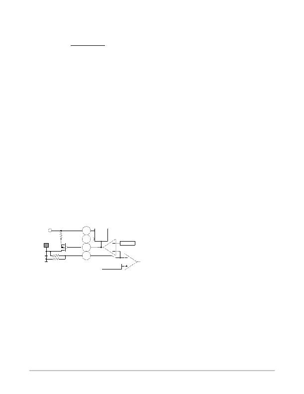
�Supply�
�output�
�ISNS� [x� ]+�
�ISNS� [x]� ?�
�LR _ G[x]�
�LR� _� FB� [x]�
�ILIMIT�
�EA�
�VREF�
�dump� condition.� If� the� input� rises� above� 16� V� (typ),� the�
�internal� gate� of� the� high� ?� side� switch� will� be� pulled� low� to�
�keep� the� source� from� rising.� The� high� ?� side� switch� will�
�operate� in� this� linear� mode� until� the� input� voltage� exceeds�
�18.5� V� (typ)� at� which� point� the� entire� IC� will� shutdown.�
�SCP�
�70%� VREF�
�Figure� 21.�
�APPLICATION� INFORMATION�
�V� OUT[x]� +� V� REF� 1� )�
�R1�
�Setting� the� Output� Voltage�
�To� set� the� output� voltage� of� any� of� the� controllers� or�
�regulators,� use� the� following� equation:�
�(eq.� 5)�
�R2�
�where,� R1� is� the� resistor� that� is� connected� from� VOUT[x]�
�to� the� feedback� pin� of� its� respective� channel� and� R2� is�
�connected� from� that� feedback� pin� to� ground.� To� reduce� the�
�effect� of� input� offset� current� error,� it� is� customary� to�
�calculate� R1� with� R2� equal� to� 1� k� W� .�
�LDO1� and� LDO2� Pass� Device� Selection�
�The� LDO� controllers� have� been� optimized� to� give� the� best�
�performance� with� the� NTD20P06L� p� ?� channel� MOSFET.�
�While� other� p� ?� channel� MOSFET� can� be� used,� specifications�
�in� the� electrical� table� are� guaranteed� only� with� the�
�NTD20P06L,� and� using� a� different� MOSFET� may� require�
�external� compensation� to� stabilize� the� output.� The�
�NTD20P06L� can� be� used� as� the� pass� device� for� both�
�controllers,� and� is� rated� with� a� ?� 60� V� max� V� DS.� This� device�
�comes� in� two� different� packages� allowing� great� flexibility�
�http://onsemi.com�
�17�
�相关PDF资料 |
PDF描述 |
|---|---|
| VE-JNF-CX-F2 | CONVERTER MOD DC/DC 72V 75W |
| TH3C106K016E1400 | CAP TANT 10UF 16V 10% 2312 |
| FMC20DRXH | CONN EDGECARD 40POS DIP .100 SLD |
| ISL6207HBZ-T | IC MOSFET DRVR SYNC BUCK 8-SOIC |
| VE-2N0-EW-B1 | CONVERTER MOD DC/DC 5V 100W |
相关代理商/技术参数 |
参数描述 |
|---|---|
| NCV8855BMNR2GEVB | 功能描述:电源管理IC开发工具 SMPS ASIC RoHS:否 制造商:Maxim Integrated 产品:Evaluation Kits 类型:Battery Management 工具用于评估:MAX17710GB 输入电压: 输出电压:1.8 V |
| NCV8870 | 制造商:ONSEMI 制造商全称:ON Semiconductor 功能描述:Automotive Grade Non-Synchronous Boost Controller |
| NCV887000 | 制造商:ONSEMI 制造商全称:ON Semiconductor 功能描述:Automotive Grade Non-Synchronous Boost Controller |
| NCV887000D1R2G | 功能描述:低压差稳压器 - LDO Auto Grade Non-Sync Boost Controller RoHS:否 制造商:Texas Instruments 最大输入电压:36 V 输出电压:1.4 V to 20.5 V 回动电压(最大值):307 mV 输出电流:1 A 负载调节:0.3 % 输出端数量: 输出类型:Fixed 最大工作温度:+ 125 C 安装风格:SMD/SMT 封装 / 箱体:VQFN-20 |
| NCV887001 | 制造商:ONSEMI 制造商全称:ON Semiconductor 功能描述:Automotive Grade Non-Synchronous Boost Controller |
发布紧急采购,3分钟左右您将得到回复。