- 您现在的位置:买卖IC网 > PDF目录20679 > NCV8855BMNR2G (ON Semiconductor)IC REG QD BUCK/LINEAR 40QFN PDF资料下载
参数资料
| 型号: | NCV8855BMNR2G |
| 厂商: | ON Semiconductor |
| 文件页数: | 9/24页 |
| 文件大小: | 0K |
| 描述: | IC REG QD BUCK/LINEAR 40QFN |
| 标准包装: | 1 |
| 拓扑: | 降压(降压)(2),线性(LDO)(2) |
| 功能: | 汽车无线电设备和仪表板电源 |
| 输出数: | 4 |
| 频率 - 开关: | 170kHz |
| 电压/电流 - 输出 1: | 控制器 |
| 电压/电流 - 输出 2: | 可调式,2.5A |
| 电压/电流 - 输出 3: | 控制器 |
| 带 LED 驱动器: | 无 |
| 带监控器: | 无 |
| 带序列发生器: | 是 |
| 电源电压: | 9 V ~ 18 V |
| 工作温度: | -40°C ~ 105°C |
| 安装类型: | 表面贴装 |
| 封装/外壳: | 40-VFQFN 裸露焊盘 |
| 供应商设备封装: | 40-QFN(6x6) |
| 包装: | 标准包装 |
| 其它名称: | NCV8855BMNR2GOSDKR |
��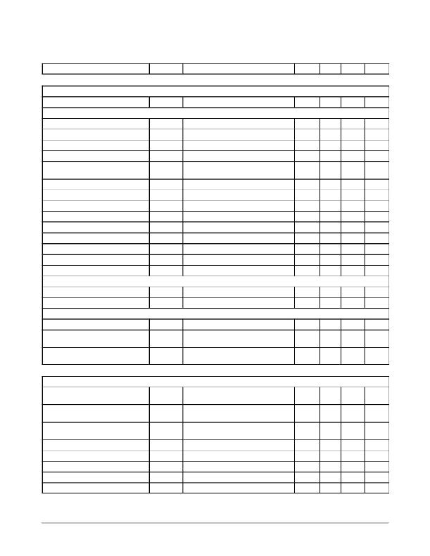 �
�
�NCV8855�
�ELECTRICAL� CHARACTERISTICS� (V� IN_SW� =� V� IN� =� V� ISNS1+� =� V� ISNS1� ?� =� V� ISNS2+� =� V� ISNS2� ?� =� 13.2� V,� SYS_EN� =� LDO_EN� =�
�HS_EN� =� 5� V,� VOUT3� =� 3.3� V,� VOUT4� =� 8.5� V,� IOUT[1:4]� =� 0� A)� Min/Max� values� are� valid� for� the� temperature� range� ?� 40� °� C� v� T� J� v�
�150� °� C� unless� noted� otherwise.� Min/Max� values� are� guaranteed� by� test,� design� or� statistical� correlation.�
�Parameter�
�Symbol�
�Conditions�
�Min�
�Typ�
�Max�
�Unit�
�SWITCH� ?� MODE� POWER� SUPPLY� REGULATOR� (SMPS2,� VOUT2)� SPECIFICATIONS�
�Internal� Soft� ?� start�
�Soft� ?� start� time�
�t� SS2�
�SYNC� floating�
�3�
�5�
�7�
�ms�
�Error� Amplifier�
�Dc� gain�
�Gain� ?� bandwidth� product�
�(Note� 1)�
�(Note� 1)�
�70�
�8�
�85�
�10�
�dB�
�MHz�
�SW_FB2� input� bias� current�
�Input� offset� voltage�
�SW_FB2� =� 0.8� V�
�100�
�500�
�800�
�nA�
�m� V�
�Slew� rate�
�COMP2� source� current�
�COMP2� sink� current�
�C� COMP2� =� 50� pF,� ±� 1� mA� dc� load� Slew� rate�
�within� ramp� voltage� levels� (Note� 1)�
�V� COMP2� =� 2.2� V�
�V� COMP2� =� 3.2� V�
�V� COMP2� =� 2.2� V�
�V� COMP2� =� 1.1� V�
�6�
�1.5�
�1.6�
�1.1�
�0.7�
�8�
�8�
�8�
�8�
�8�
�V/� m� s�
�mA�
�mA�
�mA�
�mA�
�Minimum� COMP2� voltage�
�Maximum� COMP2� voltage�
�I� COMP2� =� 500� m� A�
�I� COMP2� =� 2� mA�
�3.3�
�1.05�
�V�
�V�
�Ramp� maximum� voltage�
�Ramp� minimum� voltage�
�2.8�
�1.1�
�3.0�
�1.2�
�3.2�
�1.3�
�V�
�V�
�Ramp� voltage� amplitude�
�V� RAMP2�
�1.6�
�1.8�
�2.0�
�V�
�Duty� Cycle� Limitations�
�Minimum� off� time�
�Minimum� pulse� width�
�t� MINOFF2�
�t� MINON2�
�SN2� falling� to� SN2� rising�
�SN2� rising� to� SN2� falling,�
�80�
�120�
�140�
�250�
�200�
�300�
�ns�
�ns�
�Switching� MOSFET�
�N� ?� channel� MOSFET� R� DS(on)�
�Turn� ?� on� time�
�Turn� ?� off� time�
�T� J� =� 25� °� C,� Guaranteed� at� Probe�
�SN2� →� 0� V� to� 13.2� V,� IOUT� =� 1� A�
�(inductive� load),� T� J� =� 25� °� C�
�SN2� →� 13.2� V� to� 0� V,� IOUT� =� 1� A�
�(inductive� load),� T� J� =� 25� °� C�
�300�
�30�
�30�
�360�
�m� W�
�ns�
�ns�
�LOW� DROPOUT� LINEAR� REGULATOR� CONTROLLER� (LDO1,� VOUT3)� SPECIFICATIONS�
�Output� Voltage� Regulation�
�Output� voltage� accuracy�
�V� LR_FB1� tied� to� VOUT3� directly,�
�NTD20P06L� pass� device�
�?� 2�
�2�
�%�
�Output� voltage� line� regulation�
�Output� voltage� load� regulation�
�IOUT3� =� 10� mA,� 4.5� V� v� V� ISNS1+� v� 5.5� V,�
�NTD20P06L� pass� device�
�1� mA� v� IOUT3� v� 500� mA,� V� ISNS1+� =� 5� V,�
�NTD20P06L� pass� device�
�?� 0.25�
�?� 0.5�
�0.01�
�0.2�
�0.25�
�0.5�
�%�
�%�
�Output� load� capacitance� range�
�Output� load� capacitance� ESR� range�
�Power� supply� ripple� rejection�
�C� OUT3�
�PSRR1�
�(Note� 1)�
�(Note� 1)�
�NTD20P06L� pass� device� (Note� 1)�
�10�
�0.01�
�60�
�100�
�5�
�m� F�
�W�
�dB�
�Current� Limit�
�Current� limit� threshold� voltage�
�V� SNS1�
�V� ISNS1+� –� V� ISNS1� ?�
�90�
�110�
�130�
�mV�
�1.� Guaranteed� by� design,� not� fully� tested� in� production.�
�2.� Indirectly� guaranteed� by� test� coverage� of� other� parameters.�
�http://onsemi.com�
�9�
�相关PDF资料 |
PDF描述 |
|---|---|
| VE-JNF-CX-F2 | CONVERTER MOD DC/DC 72V 75W |
| TH3C106K016E1400 | CAP TANT 10UF 16V 10% 2312 |
| FMC20DRXH | CONN EDGECARD 40POS DIP .100 SLD |
| ISL6207HBZ-T | IC MOSFET DRVR SYNC BUCK 8-SOIC |
| VE-2N0-EW-B1 | CONVERTER MOD DC/DC 5V 100W |
相关代理商/技术参数 |
参数描述 |
|---|---|
| NCV8855BMNR2GEVB | 功能描述:电源管理IC开发工具 SMPS ASIC RoHS:否 制造商:Maxim Integrated 产品:Evaluation Kits 类型:Battery Management 工具用于评估:MAX17710GB 输入电压: 输出电压:1.8 V |
| NCV8870 | 制造商:ONSEMI 制造商全称:ON Semiconductor 功能描述:Automotive Grade Non-Synchronous Boost Controller |
| NCV887000 | 制造商:ONSEMI 制造商全称:ON Semiconductor 功能描述:Automotive Grade Non-Synchronous Boost Controller |
| NCV887000D1R2G | 功能描述:低压差稳压器 - LDO Auto Grade Non-Sync Boost Controller RoHS:否 制造商:Texas Instruments 最大输入电压:36 V 输出电压:1.4 V to 20.5 V 回动电压(最大值):307 mV 输出电流:1 A 负载调节:0.3 % 输出端数量: 输出类型:Fixed 最大工作温度:+ 125 C 安装风格:SMD/SMT 封装 / 箱体:VQFN-20 |
| NCV887001 | 制造商:ONSEMI 制造商全称:ON Semiconductor 功能描述:Automotive Grade Non-Synchronous Boost Controller |
发布紧急采购,3分钟左右您将得到回复。