- 您现在的位置:买卖IC网 > Datasheet目录490 > NTMD5836NLR2G (ON Semiconductor)MOSFET N-CH 40V 11A SO-8FL Datasheet资料下载
参数资料
| 型号: | NTMD5836NLR2G |
| 厂商: | ON Semiconductor |
| 文件页数: | 2/10页 |
| 文件大小: | 0K |
| 描述: | MOSFET N-CH 40V 11A SO-8FL |
| 标准包装: | 1 |
| FET 型: | 2 个 N 沟道(双) |
| FET 特点: | 逻辑电平门 |
| 漏极至源极电压(Vdss): | 40V |
| 电流 - 连续漏极(Id) @ 25° C: | 9A,5.7A |
| 开态Rds(最大)@ Id, Vgs @ 25° C: | 12 毫欧 @ 10A,10V |
| Id 时的 Vgs(th)(最大): | 3V @ 250µA |
| 闸电荷(Qg) @ Vgs: | 50nC @ 10V |
| 输入电容 (Ciss) @ Vds: | 2120pF @ 20V |
| 功率 - 最大: | 1.5W |
| 安装类型: | 表面贴装 |
| 封装/外壳: | 8-SOIC(0.154",3.90mm 宽) |
| 供应商设备封装: | 8-SOICN |
| 包装: | 标准包装 |
| 其它名称: | NTMD5836NLR2GOSDKR |
�� �
�
�NTMD5836NL�
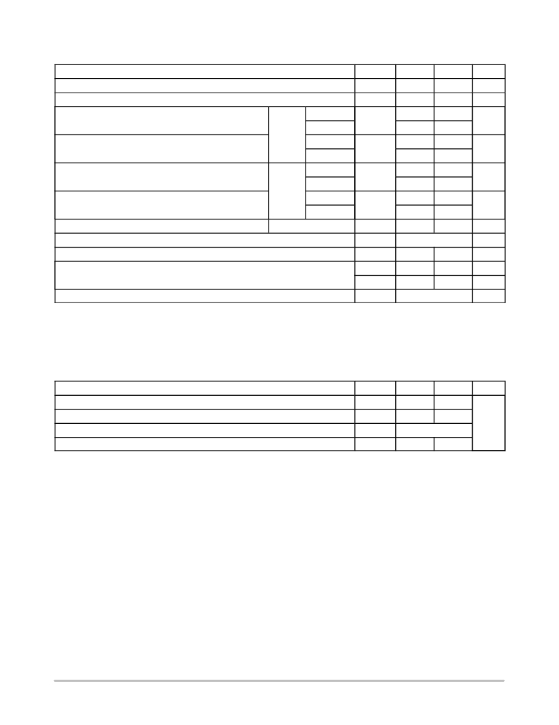
�MAXIMUM� RATINGS� (T� J� =� 25� °� C� unless� otherwise� stated)�
�Drain� ?� to� ?� Source� Voltage�
�Gate� ?� to� ?� Source� Voltage�
�Parameter�
�Symbol�
�V� DSS�
�V� GS�
�Ch� 1�
�40�
�$� 20�
�Ch� 2�
�40�
�$� 20�
�Unit�
�V�
�V�
�Continuous� Drain� Current� R� θJA� (Notes� 3� and� 4)�
�Power� Dissipation� R� θJA� (Notes� 3� and� 4)�
�Steady�
�State�
�T� A� =� 25� °� C�
�T� A� =� 70� °� C�
�T� A� =� 25� °� C�
�I� D�
�P� D�
�9.0�
�7.2�
�1.5�
�5.7�
�4.6�
�1.5�
�A�
�W�
�T� A� =� 70� °� C�
�0.9�
�0.9�
�Continuous� Drain� Current� R� θJA� (Notes� 3� and� 4)�
�t� v� 10s�
�T� A� =� 25� °� C�
�I� D�
�11�
�6.5�
�A�
�T� A� =� 70� °� C�
�8.6�
�4.6�
�Power� Dissipation� R� θJA� (Notes� 3� and� 4)�
�T� A� =� 25� °� C�
�P� D�
�2.1�
�1.9�
�W�
�T� A� =� 70� °� C�
�1.3�
�1.2�
�Pulsed� Drain� Current�
�t� p� =� 10� m� s�
�I� DM�
�43�
�26�
�A�
�Operating� Junction� and� Storage� Temperature�
�T� J� ,� T� STG�
�?� 55� to� +150�
�°� C�
�Source� Current� (Body� Diode)�
�Single� Pulse� Drain� ?� to� ?� Source� Avalanche� Energy� (V� DD� =� 40� V,� V� GS� =� 10� V,� L� =� 0.1� mH� )�
�Lead� Temperature� for� Soldering� Purposes� (1/8”� from� case� for� 10s)�
�I� S�
�E� AS�
�I� AS�
�T� L�
�10�
�76�
�39�
�260�
�7.0�
�22�
�21�
�A�
�mJ�
�A�
�°� C�
�Stresses� exceeding� Maximum� Ratings� may� damage� the� device.� Maximum� Ratings� are� stress� ratings� only.� Functional� operation� above� the�
�Recommended� Operating� Conditions� is� not� implied.� Extended� exposure� to� stresses� above� the� Recommended� Operating� Conditions� may� affect�
�device� reliability.�
�3.� Surface� ?� mounted� on� FR4� board� using� 1� in� sq� pad� size� (Cu� area� =� 1.127� in� sq� [2� oz]� including� traces)�
�4.� Only� selected� channel� is� been� powered�
�1W� applied� on� channel� 1:� T� J� =� 1� W� *� 85� °� C/W� +� 25� °� C� =� 110� °� C�
�THERMAL� RESISTANCE� RATINGS�
�Parameter�
�Junction� ?� to� ?� Ambient� Steady� State� (Notes� 5� and� 7)�
�Junction� ?� to� ?� Ambient� –� t� v� 10� s� (Notes� 5� and� 7)�
�Junction� ?� to� ?� Ambient� Steady� State� (Notes� 5� and� 8)�
�Junction� ?� to� ?� Ambient� Steady� State� (Notes� 6� and� 7)�
�Symbol�
�R� θJA�
�R� θJA�
�R� θJA�
�R� θJA�
�Ch� 1�
�85�
�60�
�136�
�59�
�Ch� 2�
�86�
�65�
�136�
�Unit�
�°� C/W�
�5.� Surface� ?� mounted� on� FR4� board� using� 1� in� sq� pad� size� (Cu� area� =� 1.127� in� sq� [2� oz]� including� traces)�
�6.� Surface� ?� mounted� on� FR4� board� using� 0.155� in� sq� (100� mm� 2� )� pad� size�
�7.� Only� selected� channel� is� been� powered�
�1W� applied� on� channel� 1:� T� J� =� 1� W� *� 85� °� C/W� +� 25� °� C� =� 110� °� C�
�8.� Both� channels� receive� equivalent� power� dissipation�
�1� W� applied� on� each� channel:� T� J� =� 2� W� *� 59� °� C/W� +� 25� °� C� =� 143� °� C�
�http://onsemi.com�
�2�
�相关PDF资料 |
PDF描述 |
|---|---|
| NTMD5838NLR2G | MOSFET N-CH 40V 8.9A 8SOIC |
| NTMD6N02R2 | MOSFET PWR N-CH DL 3.92A 20V 8SO |
| NTMD6N03R2 | MOSFET PWR N-CH DL 6A 30V 8SOIC |
| NTMD6P02R2G | MOSFET PWR P-CHAN DUAL 20V 8SOIC |
| NTMFD4901NFT1G | MOSFET N-CH DUAL 30V 8DFN |
相关代理商/技术参数 |
参数描述 |
|---|---|
| NTMD5838NL | 制造商:ONSEMI 制造商全称:ON Semiconductor 功能描述:Power MOSFET 30 V, 11.6 A, N?Channel, SO?8 Optimized Gate Charge |
| NTMD5838NLR2G | 功能描述:MOSFET NFETDPAK40V100A3.7M OHM RoHS:否 制造商:STMicroelectronics 晶体管极性:N-Channel 汲极/源极击穿电压:650 V 闸/源击穿电压:25 V 漏极连续电流:130 A 电阻汲极/源极 RDS(导通):0.014 Ohms 配置:Single 最大工作温度: 安装风格:Through Hole 封装 / 箱体:Max247 封装:Tube |
| NTMD6601NR2G | 功能描述:MOSFET NFET S08D 80V 1.4A 245mOHM RoHS:否 制造商:STMicroelectronics 晶体管极性:N-Channel 汲极/源极击穿电压:650 V 闸/源击穿电压:25 V 漏极连续电流:130 A 电阻汲极/源极 RDS(导通):0.014 Ohms 配置:Single 最大工作温度: 安装风格:Through Hole 封装 / 箱体:Max247 封装:Tube |
| NTMD6N02R2 | 功能描述:MOSFET 20V 6A N-Channel RoHS:否 制造商:STMicroelectronics 晶体管极性:N-Channel 汲极/源极击穿电压:650 V 闸/源击穿电压:25 V 漏极连续电流:130 A 电阻汲极/源极 RDS(导通):0.014 Ohms 配置:Single 最大工作温度: 安装风格:Through Hole 封装 / 箱体:Max247 封装:Tube |
| NTMD6N02R2/D | 制造商:未知厂家 制造商全称:未知厂家 功能描述:Power MOSFET 6.0 Amps, 20 Volts |
发布紧急采购,3分钟左右您将得到回复。