- 您现在的位置:买卖IC网 > PDF目录189449 > OR4E042BM416-DB (LATTICE SEMICONDUCTOR CORP) FPGA, 1296 CLBS, 380000 GATES, PBGA416 PDF资料下载
参数资料
| 型号: | OR4E042BM416-DB |
| 厂商: | LATTICE SEMICONDUCTOR CORP |
| 元件分类: | FPGA |
| 英文描述: | FPGA, 1296 CLBS, 380000 GATES, PBGA416 |
| 封装: | PLASTIC, FBGA-416 |
| 文件页数: | 112/151页 |
| 文件大小: | 2680K |
| 代理商: | OR4E042BM416-DB |
第1页第2页第3页第4页第5页第6页第7页第8页第9页第10页第11页第12页第13页第14页第15页第16页第17页第18页第19页第20页第21页第22页第23页第24页第25页第26页第27页第28页第29页第30页第31页第32页第33页第34页第35页第36页第37页第38页第39页第40页第41页第42页第43页第44页第45页第46页第47页第48页第49页第50页第51页第52页第53页第54页第55页第56页第57页第58页第59页第60页第61页第62页第63页第64页第65页第66页第67页第68页第69页第70页第71页第72页第73页第74页第75页第76页第77页第78页第79页第80页第81页第82页第83页第84页第85页第86页第87页第88页第89页第90页第91页第92页第93页第94页第95页第96页第97页第98页第99页第100页第101页第102页第103页第104页第105页第106页第107页第108页第109页第110页第111页当前第112页第113页第114页第115页第116页第117页第118页第119页第120页第121页第122页第123页第124页第125页第126页第127页第128页第129页第130页第131页第132页第133页第134页第135页第136页第137页第138页第139页第140页第141页第142页第143页第144页第145页第146页第147页第148页第149页第150页第151页
Lattice Semiconductor
63
Data Sheet
September, 2002
ORCA Series 4 FPGAs
Conguration Data Format (continued)
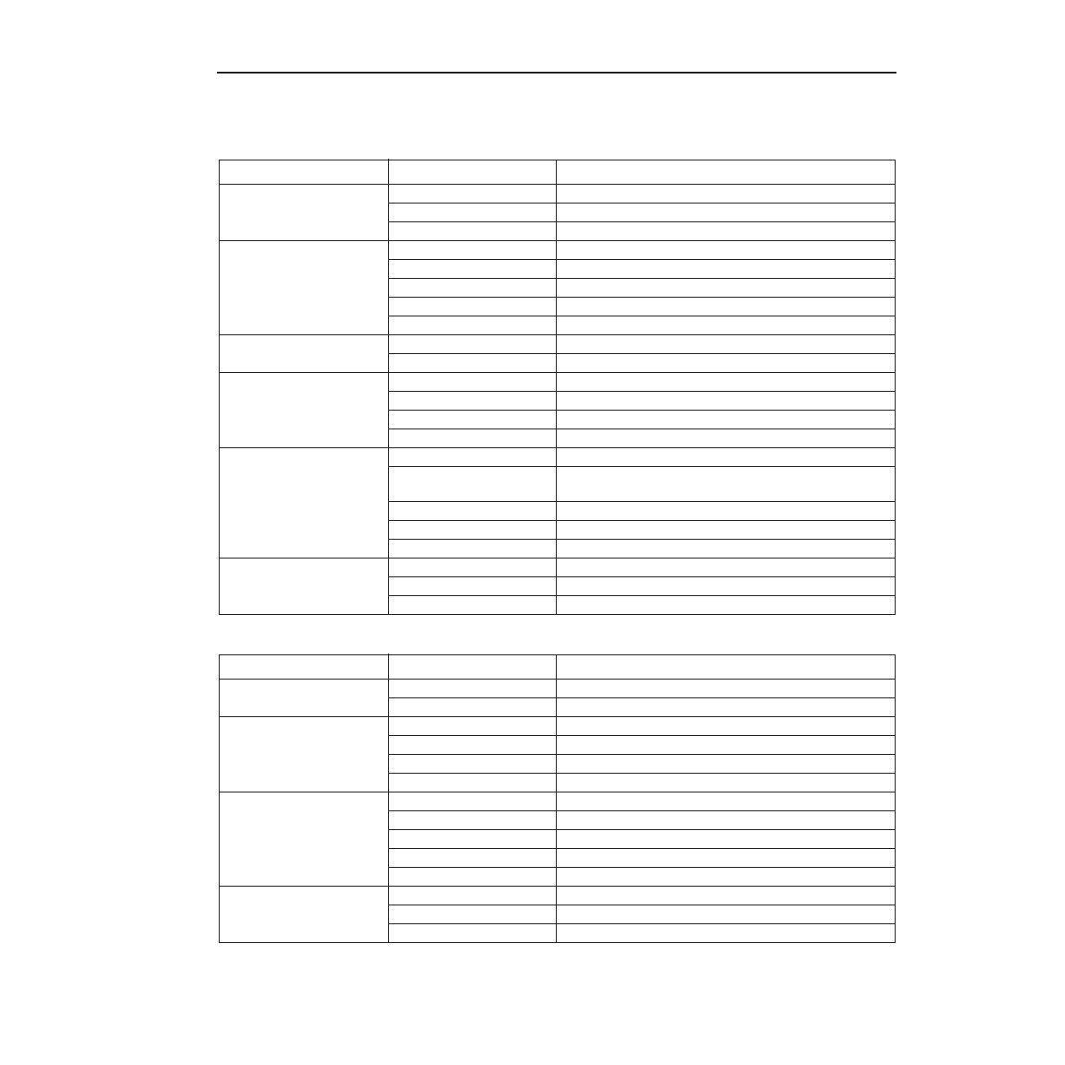
Table 31. Conguration Frame Format and Contents
Table 31A. Conguration Frame Format and Contents for Embedded Block RAM
Frame
Contents
Description
Header
11110010
Preamble for generic FPGA.
24-bit length count
Conguration bitstream length.
11111111
8-bit trailing header.
ID Frame
0101 1111 1111 1111
ID frame header.
44 reserved bits
Reserved bits set to 0.
Part ID
20-bit part ID.
Checksum
8-bit checksum.
11111111
8 stop bits (high) to separate frames.
FPGA Header
1111 0010
This is a new mandatory header for generic portion.
11111111
8 stop bits (high) to separate frames.
FPGA Address Frame
00
Address frame header.
14-bit address
14-bit address of generic FPGA.
Checksum
8-bit checksum.
11111111
Eight stop bits (high) to separate frames.
FPGA Data Frame
01
Data frame header. same as generic.
Alignment bits
String of 0 bits added to frame to reach a byte bound-
ary.
Data bits
Number of data bits depends upon device.
Checksum
8-bit checksum.
11111111
Eight stop bits (high) to separate frames.
Postamble for Generic
FPGA
00 or 10
Postamble header, 00 = nish, 10 = more bits coming.
11111111 111111
Dummy address.
11111111 11111111
16 stop bits (high).
Frame
Contents
Description
RAM Header
11110001
A mandatory header for RAM bitstream portion.
11111111
8 stop bits (high) to separate frames.
RAM Address Frame
00
Address frame header. same as generic.
6-bit address
6-bit address of RAM blocks.
Checksum
8-bit checksum.
11111111
Eight stop bits (high) to separate frames.
RAM Data Frame
01
Data frame header. same as generic.
000000
Six of 0 bits added to reach a byte boundary.
512x18 data bits
Exact number of bits in a RAM block.
Checksum
8-bit checksum.
11111111
Eight stop bits (high) to separate frames.
Postamble for RAM
00 or 10
Postamble header. 00 = nish, 10 = more bits coming.
111111
Dummy address.
11111111 11111111
16 stop bits (high).
相关PDF资料 |
PDF描述 |
|---|---|
| OR4E042BM680-DB | FPGA, 1296 CLBS, 380000 GATES, PBGA680 |
| OR4E043BA352-DB | FPGA, 1296 CLBS, 380000 GATES, PBGA352 |
| OR4E043BM416-DB | FPGA, 1296 CLBS, 380000 GATES, PBGA416 |
| OR4E043BM680-DB | FPGA, 1296 CLBS, 380000 GATES, PBGA680 |
| OR4E061BA352-DB | FPGA, 2024 CLBS, 515000 GATES, PBGA352 |
相关代理商/技术参数 |
参数描述 |
|---|---|
| OR4E04-2BM416I | 功能描述:FPGA - 现场可编程门阵列 10368 LUT 466 I/O RoHS:否 制造商:Altera Corporation 系列:Cyclone V E 栅极数量: 逻辑块数量:943 内嵌式块RAM - EBR:1956 kbit 输入/输出端数量:128 最大工作频率:800 MHz 工作电源电压:1.1 V 最大工作温度:+ 70 C 安装风格:SMD/SMT 封装 / 箱体:FBGA-256 |
| OR4E04-2BM680C | 功能描述:FPGA - 现场可编程门阵列 10368 LUT 466 I/O RoHS:否 制造商:Altera Corporation 系列:Cyclone V E 栅极数量: 逻辑块数量:943 内嵌式块RAM - EBR:1956 kbit 输入/输出端数量:128 最大工作频率:800 MHz 工作电源电压:1.1 V 最大工作温度:+ 70 C 安装风格:SMD/SMT 封装 / 箱体:FBGA-256 |
| OR4E04-2BM680I | 功能描述:FPGA - 现场可编程门阵列 10368 LUT 466 I/O RoHS:否 制造商:Altera Corporation 系列:Cyclone V E 栅极数量: 逻辑块数量:943 内嵌式块RAM - EBR:1956 kbit 输入/输出端数量:128 最大工作频率:800 MHz 工作电源电压:1.1 V 最大工作温度:+ 70 C 安装风格:SMD/SMT 封装 / 箱体:FBGA-256 |
| OR4E04-3BA352C | 功能描述:FPGA - 现场可编程门阵列 10368 LUT 466 I/O RoHS:否 制造商:Altera Corporation 系列:Cyclone V E 栅极数量: 逻辑块数量:943 内嵌式块RAM - EBR:1956 kbit 输入/输出端数量:128 最大工作频率:800 MHz 工作电源电压:1.1 V 最大工作温度:+ 70 C 安装风格:SMD/SMT 封装 / 箱体:FBGA-256 |
| OR4E04-3BM416C | 功能描述:FPGA - 现场可编程门阵列 10368 LUT 466 I/O RoHS:否 制造商:Altera Corporation 系列:Cyclone V E 栅极数量: 逻辑块数量:943 内嵌式块RAM - EBR:1956 kbit 输入/输出端数量:128 最大工作频率:800 MHz 工作电源电压:1.1 V 最大工作温度:+ 70 C 安装风格:SMD/SMT 封装 / 箱体:FBGA-256 |
发布紧急采购,3分钟左右您将得到回复。