- 您现在的位置:买卖IC网 > PDF目录189449 > OR4E042BM416-DB (LATTICE SEMICONDUCTOR CORP) FPGA, 1296 CLBS, 380000 GATES, PBGA416 PDF资料下载
参数资料
| 型号: | OR4E042BM416-DB |
| 厂商: | LATTICE SEMICONDUCTOR CORP |
| 元件分类: | FPGA |
| 英文描述: | FPGA, 1296 CLBS, 380000 GATES, PBGA416 |
| 封装: | PLASTIC, FBGA-416 |
| 文件页数: | 71/151页 |
| 文件大小: | 2680K |
| 代理商: | OR4E042BM416-DB |
第1页第2页第3页第4页第5页第6页第7页第8页第9页第10页第11页第12页第13页第14页第15页第16页第17页第18页第19页第20页第21页第22页第23页第24页第25页第26页第27页第28页第29页第30页第31页第32页第33页第34页第35页第36页第37页第38页第39页第40页第41页第42页第43页第44页第45页第46页第47页第48页第49页第50页第51页第52页第53页第54页第55页第56页第57页第58页第59页第60页第61页第62页第63页第64页第65页第66页第67页第68页第69页第70页当前第71页第72页第73页第74页第75页第76页第77页第78页第79页第80页第81页第82页第83页第84页第85页第86页第87页第88页第89页第90页第91页第92页第93页第94页第95页第96页第97页第98页第99页第100页第101页第102页第103页第104页第105页第106页第107页第108页第109页第110页第111页第112页第113页第114页第115页第116页第117页第118页第119页第120页第121页第122页第123页第124页第125页第126页第127页第128页第129页第130页第131页第132页第133页第134页第135页第136页第137页第138页第139页第140页第141页第142页第143页第144页第145页第146页第147页第148页第149页第150页第151页
26
Lattice Semiconductor
Data Sheet
September, 2002
ORCA Series 4 FPGAs
Embedded Block RAM (EBR)
The ORCA Series 4 devices compliment the distributed
PFU RAM with large blocks of memory macrocells. The
memory is available in 512 words by 18 bits/word
blocks with 2 read and 2 write ports with two byte lane
enables which operate with quad-port functionality.
Additional logic has been incorporated for FIFO, multi-
plier, and CAM implementations. The RAM blocks are
organized along the PLC rows and are added in pro-
portion to the FPGA array sizes as shown in Table 7.
The contents of the RAM blocks may be optionally ini-
tialized during FPGA conguration.
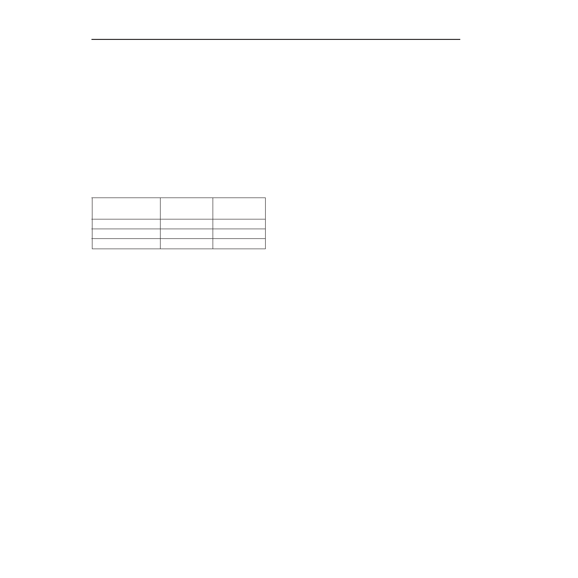
Table 7. ORCA Series 4— Available Embedded
Block RAM
Each highly exible 512x18 (quad-port, two read/two
write) RAM block can be programmed by the user to
meet their particular function. Each of the EBR congu-
rations use the physical signals as shown in
Table 8. Quad-port addressing permits simultaneous
read and write operations on all four ports.
The EBR ports are written synchronously on the posi-
tive-edge of CKW. Synchronous read operations uses
the positive-edge of CKR. Options are available to use
synchronous read address registers and read output
registers, or to bypass these registers and have the
RAM read operate asynchronously. Detailed informa-
tion about the EBR blocks is found in various applica-
tion notes.
ORCA Foundry provides SCUBA as a RAM generation
tool for EBR RAMs. Many of the EBR sub-modes are
supported and the initialization values can also be
dened.
EBR Features
Quad Port RAM Modes (Two Read/Two Write)
■
One 512 x 18 RAM with optional built-in write arbitra-
tion.
■
One 1024 x 18 RAM built on two blocks with built-in
decode logic for simplied implementation.
Dual Port RAM Modes (One Read/One Write)
■
One 256 x 36 RAM.
■
One 1K x 9 RAM.
■
Two independent 512 x 9 RAMs built in one EBR with
separate read clocks, write clocks and enables.
■
Two independent RAMS with arbitrary number of
words whose sum is 512 words or less by 18 bits/
word or less.
The joining of RAM blocks is supported to create wider
deeper memories. The adjacent routing interface pro-
vided by the CIBs allow the cascading of blocks
together with minimal penalties due to routing delays.
It is also possible to connect any or all of the EBR RAM
blocks together through the embedded system bus,
which is discussed in a later section of this data sheet.
Arbitration logic is optionally programmed by the user
to signal occurrences of data collisions as well as to
block both ports from writing at the same time. The
arbitration logic prioritizes PORT1. When utilizing the
arbiter, the signal BUSY indicates data is being written
to PORT1. This BUSY output signals PORT1 activity by
driving a high output. If the arbiter is turned off both
ports could be written at the same time and the data
would be corrupt. In this scenario the BUSY signal will
indicate a possible error.
There is also a user option which dedicates PORT 1 to
communications to the system bus. In this mode the
user logic only has access to PORT0 and arbitration
logic is enabled. The system bus utilizes the priority
given to it by the arbiter therefore the system bus will
always be able to write to the EBR.
Device
Number of
Blocks
Number of
EBR Bits
OR4E02
8
74K
OR4E04
12
111K
OR4E06
16
147K
相关PDF资料 |
PDF描述 |
|---|---|
| OR4E042BM680-DB | FPGA, 1296 CLBS, 380000 GATES, PBGA680 |
| OR4E043BA352-DB | FPGA, 1296 CLBS, 380000 GATES, PBGA352 |
| OR4E043BM416-DB | FPGA, 1296 CLBS, 380000 GATES, PBGA416 |
| OR4E043BM680-DB | FPGA, 1296 CLBS, 380000 GATES, PBGA680 |
| OR4E061BA352-DB | FPGA, 2024 CLBS, 515000 GATES, PBGA352 |
相关代理商/技术参数 |
参数描述 |
|---|---|
| OR4E04-2BM416I | 功能描述:FPGA - 现场可编程门阵列 10368 LUT 466 I/O RoHS:否 制造商:Altera Corporation 系列:Cyclone V E 栅极数量: 逻辑块数量:943 内嵌式块RAM - EBR:1956 kbit 输入/输出端数量:128 最大工作频率:800 MHz 工作电源电压:1.1 V 最大工作温度:+ 70 C 安装风格:SMD/SMT 封装 / 箱体:FBGA-256 |
| OR4E04-2BM680C | 功能描述:FPGA - 现场可编程门阵列 10368 LUT 466 I/O RoHS:否 制造商:Altera Corporation 系列:Cyclone V E 栅极数量: 逻辑块数量:943 内嵌式块RAM - EBR:1956 kbit 输入/输出端数量:128 最大工作频率:800 MHz 工作电源电压:1.1 V 最大工作温度:+ 70 C 安装风格:SMD/SMT 封装 / 箱体:FBGA-256 |
| OR4E04-2BM680I | 功能描述:FPGA - 现场可编程门阵列 10368 LUT 466 I/O RoHS:否 制造商:Altera Corporation 系列:Cyclone V E 栅极数量: 逻辑块数量:943 内嵌式块RAM - EBR:1956 kbit 输入/输出端数量:128 最大工作频率:800 MHz 工作电源电压:1.1 V 最大工作温度:+ 70 C 安装风格:SMD/SMT 封装 / 箱体:FBGA-256 |
| OR4E04-3BA352C | 功能描述:FPGA - 现场可编程门阵列 10368 LUT 466 I/O RoHS:否 制造商:Altera Corporation 系列:Cyclone V E 栅极数量: 逻辑块数量:943 内嵌式块RAM - EBR:1956 kbit 输入/输出端数量:128 最大工作频率:800 MHz 工作电源电压:1.1 V 最大工作温度:+ 70 C 安装风格:SMD/SMT 封装 / 箱体:FBGA-256 |
| OR4E04-3BM416C | 功能描述:FPGA - 现场可编程门阵列 10368 LUT 466 I/O RoHS:否 制造商:Altera Corporation 系列:Cyclone V E 栅极数量: 逻辑块数量:943 内嵌式块RAM - EBR:1956 kbit 输入/输出端数量:128 最大工作频率:800 MHz 工作电源电压:1.1 V 最大工作温度:+ 70 C 安装风格:SMD/SMT 封装 / 箱体:FBGA-256 |
发布紧急采购,3分钟左右您将得到回复。