- 您现在的位置:买卖IC网 > PDF目录189449 > OR4E042BM416-DB (LATTICE SEMICONDUCTOR CORP) FPGA, 1296 CLBS, 380000 GATES, PBGA416 PDF资料下载
参数资料
| 型号: | OR4E042BM416-DB |
| 厂商: | LATTICE SEMICONDUCTOR CORP |
| 元件分类: | FPGA |
| 英文描述: | FPGA, 1296 CLBS, 380000 GATES, PBGA416 |
| 封装: | PLASTIC, FBGA-416 |
| 文件页数: | 69/151页 |
| 文件大小: | 2680K |
| 代理商: | OR4E042BM416-DB |
第1页第2页第3页第4页第5页第6页第7页第8页第9页第10页第11页第12页第13页第14页第15页第16页第17页第18页第19页第20页第21页第22页第23页第24页第25页第26页第27页第28页第29页第30页第31页第32页第33页第34页第35页第36页第37页第38页第39页第40页第41页第42页第43页第44页第45页第46页第47页第48页第49页第50页第51页第52页第53页第54页第55页第56页第57页第58页第59页第60页第61页第62页第63页第64页第65页第66页第67页第68页当前第69页第70页第71页第72页第73页第74页第75页第76页第77页第78页第79页第80页第81页第82页第83页第84页第85页第86页第87页第88页第89页第90页第91页第92页第93页第94页第95页第96页第97页第98页第99页第100页第101页第102页第103页第104页第105页第106页第107页第108页第109页第110页第111页第112页第113页第114页第115页第116页第117页第118页第119页第120页第121页第122页第123页第124页第125页第126页第127页第128页第129页第130页第131页第132页第133页第134页第135页第136页第137页第138页第139页第140页第141页第142页第143页第144页第145页第146页第147页第148页第149页第150页第151页
24
Lattice Semiconductor
Data Sheet
September, 2002
ORCA Series 4 FPGAs
Programmable Logic Cells (continued)
5-5748(F)
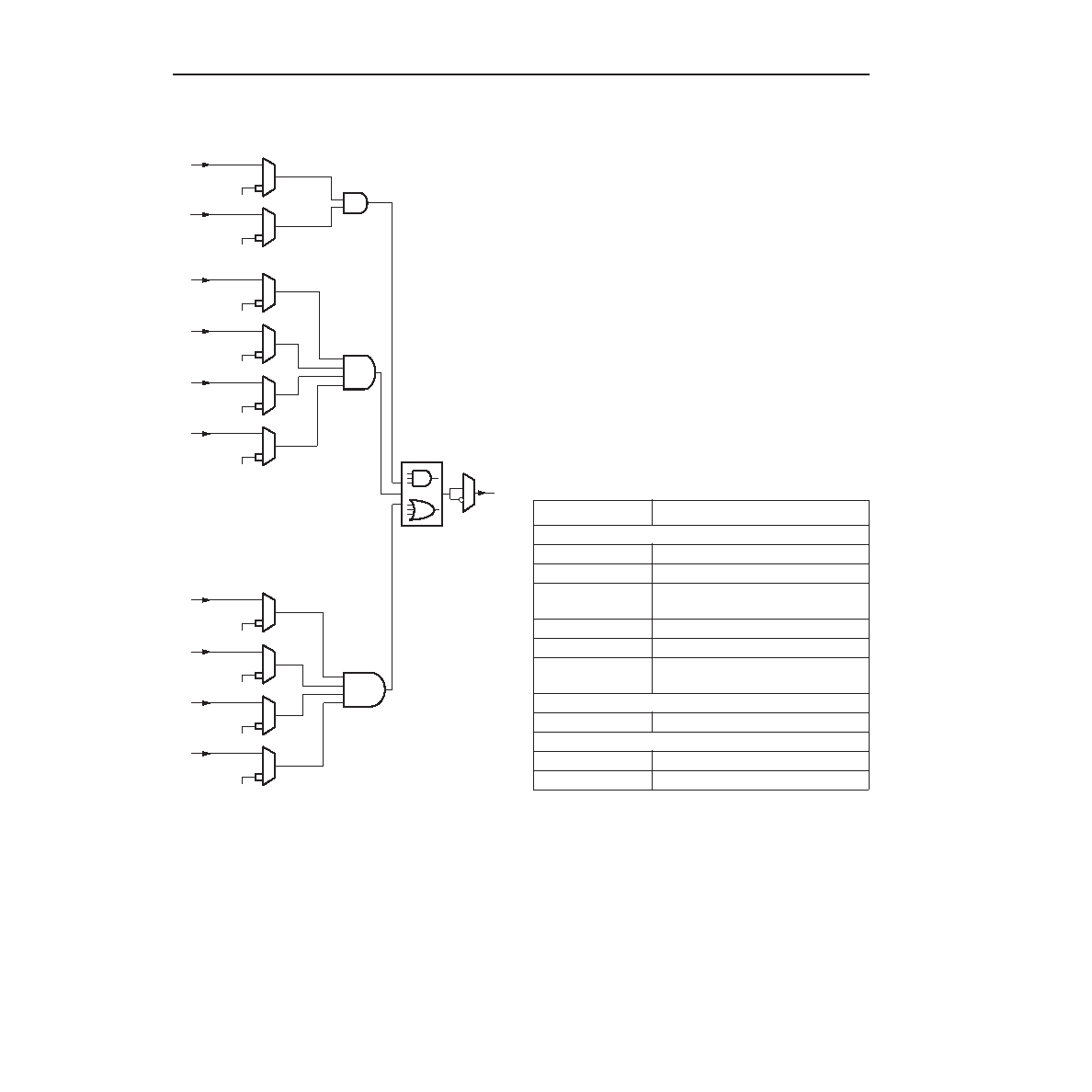
Figure 19. Decoder Mode
PLC Latches/Flip-Flops
The eight general-purpose latches/FFs in the PFU can
be used in a variety of congurations. In some cases,
the conguration options apply to all eight latches/FFs
in the PFU and some apply to the latches/FFs on a nib-
ble-wide basis where the ninth FF is considered inde-
pendently. For other options, each latch/FF is
independently programmable. In addition, the ninth FF
can be used for a variety of functions.
Table 6 summarizes these latch/FF options. The
latches/FFs can be congured as either positive- or
negative-level sensitive latches, or positive or negative
edge-triggered FFs (the ninth register can only be a
FF). All latches/FFs in a given PFU share the same
clock, and the clock to these latches/FFs can be
inverted. The input into each latch/FF is from either the
corresponding LUT output (F[7:0]) or the direct data
input (DIN[7:0]). The latch/FF input can also be tied to
logic 1 or to logic 0, which is the default.
Table 6. Conguration RAM Controlled Latch/
Flip-Flop Operation
Each PFU has two independent programmable clocks,
clock enable CE[1:0], local set/reset LSR[1:0], and
front end data selects SEL[1:0]. When CE is disabled,
each latch/FF retains its previous value when clocked.
The clock enable, LSR, and SEL inputs can be inverted
to be active-low.
DEC
SIN7
LOGIC 1 OR 0
SIN6
LOGIC 1 OR 0
SIN5
LOGIC 1 OR 0
SIN4
LOGIC 1 OR 0
SIN9
LOGIC 1 OR 0
SIN8
LOGIC 1 OR 0
SIN3
LOGIC 1 OR 0
SIN1
LOGIC 1 OR 0
SIN2
LOGIC 1 OR 0
SIN0
LOGIC 1 OR 0
Function
Options
Common to All Latches/FFs in PFU
LSR Operation
Asynchronous or synchronous.
Clock Polarity
Noninverted or inverted.
Front-end Select* Direct (DIN[7:0]) or from LUT
(F[7:0]).
LSR Priority
Either LSR or CE has priority.
Latch/FF Mode
Latch or FF.
Enable GSRN
GSRN enabled or has no effect on
PFU latches/FFs.
Set Individually in Each Latch/FF in PFU
Set/Reset Mode
Set or reset.
By Group (Latch/FF[3:0], Latch/FF[7:4], and FF[8])
Clock Enable
CE or none.
LSR Control
LSR or none.
* Not available for FF[8].
相关PDF资料 |
PDF描述 |
|---|---|
| OR4E042BM680-DB | FPGA, 1296 CLBS, 380000 GATES, PBGA680 |
| OR4E043BA352-DB | FPGA, 1296 CLBS, 380000 GATES, PBGA352 |
| OR4E043BM416-DB | FPGA, 1296 CLBS, 380000 GATES, PBGA416 |
| OR4E043BM680-DB | FPGA, 1296 CLBS, 380000 GATES, PBGA680 |
| OR4E061BA352-DB | FPGA, 2024 CLBS, 515000 GATES, PBGA352 |
相关代理商/技术参数 |
参数描述 |
|---|---|
| OR4E04-2BM416I | 功能描述:FPGA - 现场可编程门阵列 10368 LUT 466 I/O RoHS:否 制造商:Altera Corporation 系列:Cyclone V E 栅极数量: 逻辑块数量:943 内嵌式块RAM - EBR:1956 kbit 输入/输出端数量:128 最大工作频率:800 MHz 工作电源电压:1.1 V 最大工作温度:+ 70 C 安装风格:SMD/SMT 封装 / 箱体:FBGA-256 |
| OR4E04-2BM680C | 功能描述:FPGA - 现场可编程门阵列 10368 LUT 466 I/O RoHS:否 制造商:Altera Corporation 系列:Cyclone V E 栅极数量: 逻辑块数量:943 内嵌式块RAM - EBR:1956 kbit 输入/输出端数量:128 最大工作频率:800 MHz 工作电源电压:1.1 V 最大工作温度:+ 70 C 安装风格:SMD/SMT 封装 / 箱体:FBGA-256 |
| OR4E04-2BM680I | 功能描述:FPGA - 现场可编程门阵列 10368 LUT 466 I/O RoHS:否 制造商:Altera Corporation 系列:Cyclone V E 栅极数量: 逻辑块数量:943 内嵌式块RAM - EBR:1956 kbit 输入/输出端数量:128 最大工作频率:800 MHz 工作电源电压:1.1 V 最大工作温度:+ 70 C 安装风格:SMD/SMT 封装 / 箱体:FBGA-256 |
| OR4E04-3BA352C | 功能描述:FPGA - 现场可编程门阵列 10368 LUT 466 I/O RoHS:否 制造商:Altera Corporation 系列:Cyclone V E 栅极数量: 逻辑块数量:943 内嵌式块RAM - EBR:1956 kbit 输入/输出端数量:128 最大工作频率:800 MHz 工作电源电压:1.1 V 最大工作温度:+ 70 C 安装风格:SMD/SMT 封装 / 箱体:FBGA-256 |
| OR4E04-3BM416C | 功能描述:FPGA - 现场可编程门阵列 10368 LUT 466 I/O RoHS:否 制造商:Altera Corporation 系列:Cyclone V E 栅极数量: 逻辑块数量:943 内嵌式块RAM - EBR:1956 kbit 输入/输出端数量:128 最大工作频率:800 MHz 工作电源电压:1.1 V 最大工作温度:+ 70 C 安装风格:SMD/SMT 封装 / 箱体:FBGA-256 |
发布紧急采购,3分钟左右您将得到回复。