- 您现在的位置:买卖IC网 > PDF目录189449 > OR4E043BM416-DB (LATTICE SEMICONDUCTOR CORP) FPGA, 1296 CLBS, 380000 GATES, PBGA416 PDF资料下载
参数资料
| 型号: | OR4E043BM416-DB |
| 厂商: | LATTICE SEMICONDUCTOR CORP |
| 元件分类: | FPGA |
| 英文描述: | FPGA, 1296 CLBS, 380000 GATES, PBGA416 |
| 封装: | PLASTIC, FBGA-416 |
| 文件页数: | 104/151页 |
| 文件大小: | 2680K |
| 代理商: | OR4E043BM416-DB |
第1页第2页第3页第4页第5页第6页第7页第8页第9页第10页第11页第12页第13页第14页第15页第16页第17页第18页第19页第20页第21页第22页第23页第24页第25页第26页第27页第28页第29页第30页第31页第32页第33页第34页第35页第36页第37页第38页第39页第40页第41页第42页第43页第44页第45页第46页第47页第48页第49页第50页第51页第52页第53页第54页第55页第56页第57页第58页第59页第60页第61页第62页第63页第64页第65页第66页第67页第68页第69页第70页第71页第72页第73页第74页第75页第76页第77页第78页第79页第80页第81页第82页第83页第84页第85页第86页第87页第88页第89页第90页第91页第92页第93页第94页第95页第96页第97页第98页第99页第100页第101页第102页第103页当前第104页第105页第106页第107页第108页第109页第110页第111页第112页第113页第114页第115页第116页第117页第118页第119页第120页第121页第122页第123页第124页第125页第126页第127页第128页第129页第130页第131页第132页第133页第134页第135页第136页第137页第138页第139页第140页第141页第142页第143页第144页第145页第146页第147页第148页第149页第150页第151页
56
Lattice Semiconductor
Data Sheet
September, 2002
ORCA Series 4 FPGAs
FPGA States of Operation
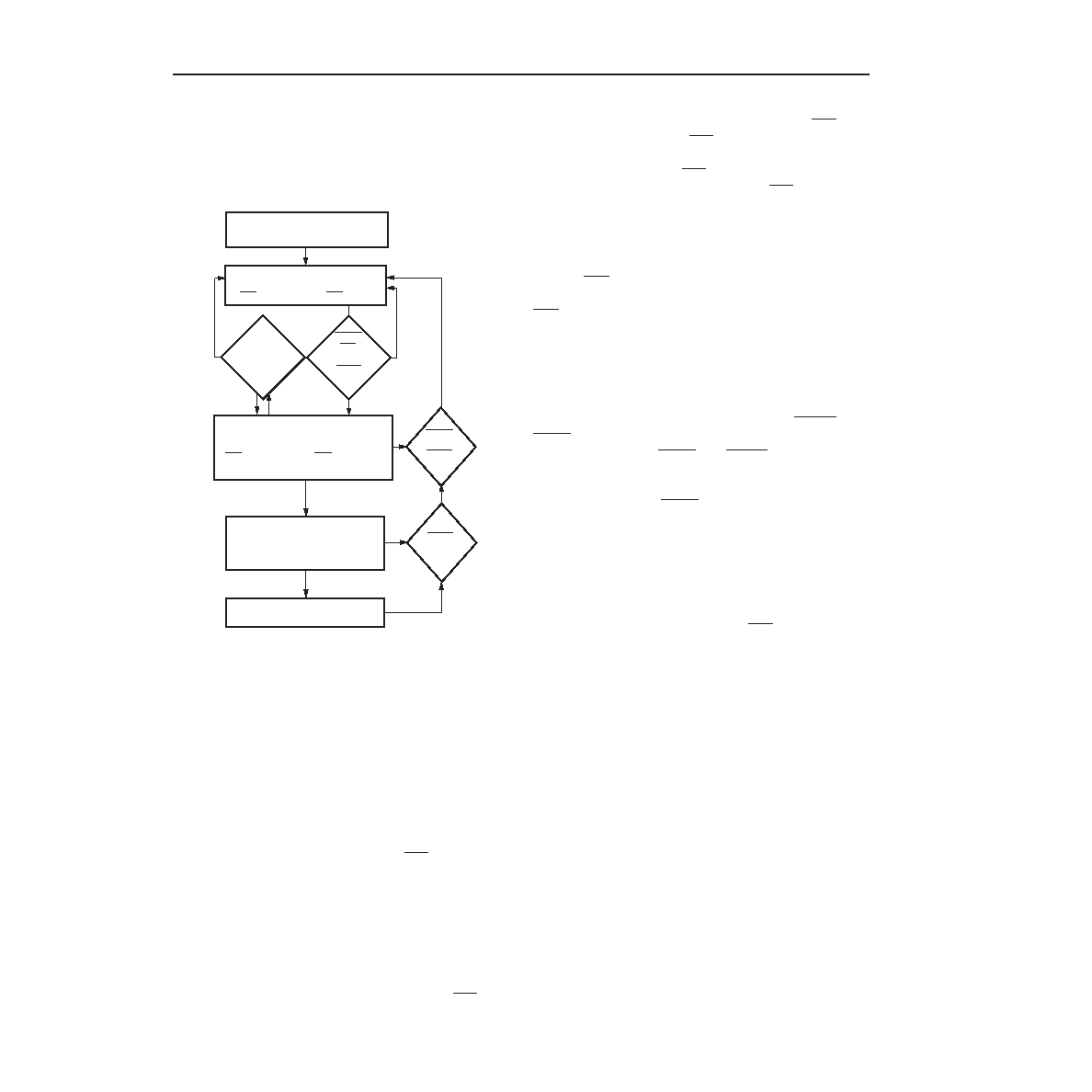
Prior to becoming operational, the FPGA goes through
a sequence of states, including initialization, congura-
tion, and start-up. Figure 33 outlines these three states.
5-4529(F).
Figure 33. FPGA States of Operation
Initialization
Upon powerup, the device goes through an initialization
process. First, an internal power-on-reset circuit is trig-
gered when power is applied. When VDD15 and VDD33
reach the voltage at which portions of the FPGA begin
to operate, the I/Os are congured based on the cong-
uration mode, as determined by the mode select inputs
M[3:0]. A time-out delay is then initiated to allow the
power supply voltage to stabilize. The INIT and DONE
outputs are low.
At the end of initialization, the default conguration
option is that the conguration RAM is written to a low
state. This prevents internal shorts prior to congura-
tion. As a conguration option, after the rst congura-
tion (i.e., at reconguration), the user can recongure
without clearing the internal conguration RAM rst.
The active-low, open-drain initialization signal INIT is
released and must be pulled high by an external resis-
tor when initialization is complete. To synchronize the
conguration of multiple FPGAs, one or more INIT pins
should be wire-ANDed. If INIT is held low by one or
more FPGAs or an external device, the FPGA remains
in the initialization state. INIT can be used to signal that
the FPGAs are not yet initialized. After INIT goes high
for two internal clock cycles, the mode lines (M[3:0])
are sampled, and the FPGA enters the conguration
state.
The high during conguration (HDC), low during cong-
uration (LDC), and DONE signals are active outputs in
the FPGA’s initialization and conguration states. HDC,
LDC
, and DONE can be used to provide control of
external logic signals such as reset, bus enable, or
PROM enable during conguration. For parallel master
conguration modes, these signals provide PROM
enable control and allow the data pins to be shared
with user logic signals.
If conguration has begun, an assertion of RESET or
PRGM
initiates an abort, returning the FPGA to the ini-
tialization state. The PRGM and RESET pins must be
pulled back high before the FPGA will enter the cong-
uration state. During the start-up and operating states,
only the assertion of PRGM causes a reconguration.
In the master conguration modes, the FPGA is the
source of conguration clock (CCLK). In this mode, the
initialization state is extended to ensure that, in daisy-
chain operation, all daisy-chained slave devices are
ready. Independent of differences in clock rates, master
mode devices remain in the initialization state an addi-
tional six internal clock cycles after INIT goes high.
When conguration is initiated, a counter in the FPGA
is set to 0 and begins to count conguration clock
cycles applied to the FPGA. As each conguration data
frame is supplied to the FPGA, it is internally assem-
bled into data words. Each data word is loaded into the
internal conguration memory. The conguration load-
ing process is complete when the internal length count
equals the loaded length count in the length count eld,
and the required end of conguration frame is written.
During conguration, the PIO and PLC latches/FFs are
held set/reset and the internal SLIC buffers are
3-stated. The combinatorial logic begins to function as
the FPGA is congured. Figure 34 shows the general
waveform of the initialization, conguration, and start-
up states.
– ACTIVE I/O
– RELEASE INTERNAL RESET
– DONE GOES HIGH
START-UP
INITIALIZATION
CONFIGURATION
RESET
OR
PRGM
LOW
PRGM
LOW
– CLEAR CONFIGURATION MEMORY
– INIT LOW, HDC HIGH, LDC LOW
OPERATION
POWERUP
– POWER-ON TIME DELAY
– M[3:0] MODE IS SELECTED
– CONFIGURATION DATA FRAME WRITTEN
– INIT HIGH, HDC HIGH, LDC LOW
– DOUT ACTIVE
YES
NO
RESET,
INIT,
OR
PRGM
LOW
BIT
ERROR
YES
相关PDF资料 |
PDF描述 |
|---|---|
| OR4E043BM680-DB | FPGA, 1296 CLBS, 380000 GATES, PBGA680 |
| OR4E061BA352-DB | FPGA, 2024 CLBS, 515000 GATES, PBGA352 |
| OR4E061BM680-DB | FPGA, 2024 CLBS, 515000 GATES, PBGA680 |
| OR4E062BA352-DB | FPGA, 2024 CLBS, 515000 GATES, PBGA352 |
| OR4E062BM680-DB | FPGA, 2024 CLBS, 515000 GATES, PBGA680 |
相关代理商/技术参数 |
参数描述 |
|---|---|
| OR4E04-3BM680C | 功能描述:FPGA - 现场可编程门阵列 10368 LUT 466 I/O RoHS:否 制造商:Altera Corporation 系列:Cyclone V E 栅极数量: 逻辑块数量:943 内嵌式块RAM - EBR:1956 kbit 输入/输出端数量:128 最大工作频率:800 MHz 工作电源电压:1.1 V 最大工作温度:+ 70 C 安装风格:SMD/SMT 封装 / 箱体:FBGA-256 |
| OR4E06 | 制造商:LATTICE 制造商全称:Lattice Semiconductor 功能描述:ORCASeries 4 FPGAs |
| OR4E06-1BA352C | 功能描述:FPGA - 现场可编程门阵列 16192 LUT 466 I/O RoHS:否 制造商:Altera Corporation 系列:Cyclone V E 栅极数量: 逻辑块数量:943 内嵌式块RAM - EBR:1956 kbit 输入/输出端数量:128 最大工作频率:800 MHz 工作电源电压:1.1 V 最大工作温度:+ 70 C 安装风格:SMD/SMT 封装 / 箱体:FBGA-256 |
| OR4E06-1BA352I | 功能描述:FPGA - 现场可编程门阵列 16192 LUT 466 I/O RoHS:否 制造商:Altera Corporation 系列:Cyclone V E 栅极数量: 逻辑块数量:943 内嵌式块RAM - EBR:1956 kbit 输入/输出端数量:128 最大工作频率:800 MHz 工作电源电压:1.1 V 最大工作温度:+ 70 C 安装风格:SMD/SMT 封装 / 箱体:FBGA-256 |
| OR4E06-1BM680C | 功能描述:FPGA - 现场可编程门阵列 16192 LUT 466 I/O RoHS:否 制造商:Altera Corporation 系列:Cyclone V E 栅极数量: 逻辑块数量:943 内嵌式块RAM - EBR:1956 kbit 输入/输出端数量:128 最大工作频率:800 MHz 工作电源电压:1.1 V 最大工作温度:+ 70 C 安装风格:SMD/SMT 封装 / 箱体:FBGA-256 |
发布紧急采购,3分钟左右您将得到回复。