- 您现在的位置:买卖IC网 > PDF目录11733 > ORT82G5-1FN680I (Lattice Semiconductor Corporation)IC TRANCEIVERS FPSC 680FPBGA PDF资料下载
参数资料
| 型号: | ORT82G5-1FN680I |
| 厂商: | Lattice Semiconductor Corporation |
| 文件页数: | 29/119页 |
| 文件大小: | 0K |
| 描述: | IC TRANCEIVERS FPSC 680FPBGA |
| 产品变化通告: | Product Discontinuation 01/Aug/2011 |
| 标准包装: | 24 |
| 系列: | * |
第1页第2页第3页第4页第5页第6页第7页第8页第9页第10页第11页第12页第13页第14页第15页第16页第17页第18页第19页第20页第21页第22页第23页第24页第25页第26页第27页第28页当前第29页第30页第31页第32页第33页第34页第35页第36页第37页第38页第39页第40页第41页第42页第43页第44页第45页第46页第47页第48页第49页第50页第51页第52页第53页第54页第55页第56页第57页第58页第59页第60页第61页第62页第63页第64页第65页第66页第67页第68页第69页第70页第71页第72页第73页第74页第75页第76页第77页第78页第79页第80页第81页第82页第83页第84页第85页第86页第87页第88页第89页第90页第91页第92页第93页第94页第95页第96页第97页第98页第99页第100页第101页第102页第103页第104页第105页第106页第107页第108页第109页第110页第111页第112页第113页第114页第115页第116页第117页第118页第119页
Lattice Semiconductor
ORCA ORT42G5 and ORT82G5 Data Sheet
17
Embedded Core/FPGA Logic Interface and 4:1 Multiplexer
These blocks provide the data formatting and transmit data and clock signal transfers between the Embedded Core
and the FPGA Logic. Control and status registers in the FPGA portion of the chip contain to control the transmit
logic and record status. These bits are passed to the core using the FPGA System Bus and are described in later
sections of this data sheet.
The low-speed transmit interface consists of a clock and 4 data bytes, each with an accompanying control bit. The
data bytes are conveyed to the MUX via the TWDxx[31:0] ports (where xx represents the channel label [AA,...,BD]
or [AC, AD, BC, BD]). The control bits are TCOMMAx[3:0] which dene whether the input byte is to be interpreted
as data or as a special character and TBIT9xx[3:0] which are used to force a negative disparity present state. The
data and control signals are synchronized to the transmit clock, TSYS_CLK_xx. Both the data and control are
strobed into the core on the rising edge of TSYS_CLK_xx. Note that each TBIT9xx[3:0] controls the disparity of the
encoded version of its corresponding data byte. Setting bit TBIT9AC[3] to 1, for instance, will force the 8b/10b
encoder to assess a current negative running disparity state. This will cause it to encode TWDAC[31:24] positively
(more 1’s than 0’s). Setting TBIT9xx to 0 will leave the encoder free to alternate between positive and negative
encoding to maintain a zero running disparity.
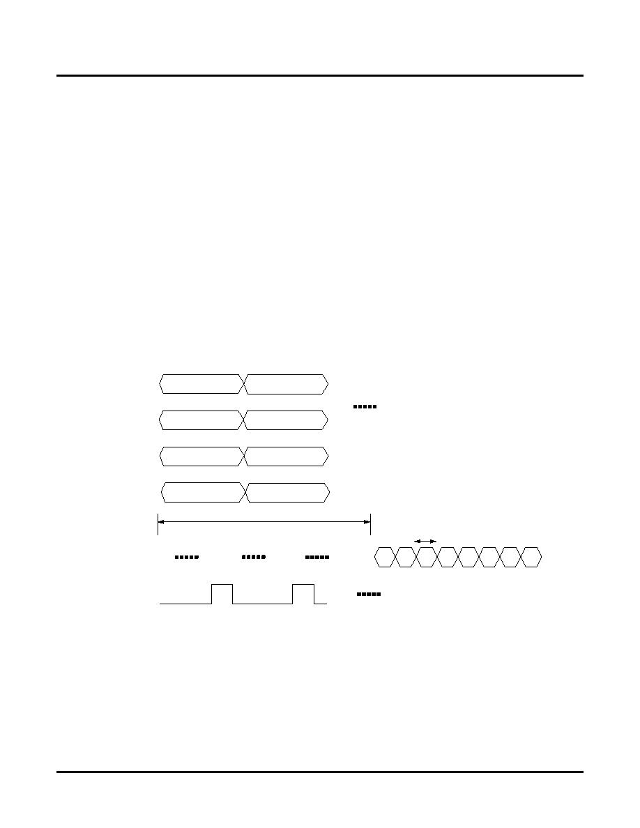
The MUX is responsible for taking 40 bits of data/control at the low-speed transmit interface and up-converting it to
10 bits of data/control at the SERDES transmit interface. The MUX has 2 clock domains - one based on the clock
received from the SERDES block and a second that comes from the FPGA at 1/4 the frequency of the SERDES
clock. The time sequence of interleaving data/control values is shown in Figure 4.
Figure 4. Transmit MUX Block Timing - Single Channel
SERDES Block
The SERDES block accepts either 8-bit data to be encoded or 10-bit unencoded data at the parallel input port from
the MUX/DEMUX block. It also accepts the reference clock at the REFCLK_[A:B] input and uses this clock to syn-
thesize the internal high-speed serial bit clock.
The internal STBC311xx clock is derived from the reference clock. The frequency of this clock depends on the set-
ting of the half-rate/full-rate control bit setting the mode of the SERDES and the frequency of the REFCLK_[A:B]
and/or that of the high-speed serial data. A falling edge on the STBC311xx clock port will cause a new data charac-
ter to be transferred into the SERDES block. The latency from the SERDES block input to the high-speed serial
output is 5 STBC311xx clock cycles, as shown in Figure 5.
p
q
r
s
t
xyz
STBDxx[9:0]
LATENCY = 4 TSYS_CLK_xx CLOCKS
TWDxx[31:24],
TSYS_CLK_xx
s
8
r
8
z
8
y
8
10-bit wide data
TWDxx[23:16],
TWDxx[15:8],
r
7-0,
y
7-0,
TCOMMAxx[3]
TCOMMAxx[2]
TCOMMAxx[1]
TCOMMAxx[0]
TWDxx[7:0],
s
7-0,
z
7-0,
TBIT9xx[0]
TBIT9xx[1]
TBIT9xx[2]
TBIT9xx[3]
q
9
r
9
s
9
z
9
y
9
x
9
p
7-0,
p
8
t
7-0,
q
8
t
8
x
8
q
7-0,
x
7-0,
p
9
t
9
相关PDF资料 |
PDF描述 |
|---|---|
| ORT82G5-2FN680I | IC TRANCEIVERS FPSC 680FPBGA |
| VI-J4H-IW-F4 | CONVERTER MOD DC/DC 52V 100W |
| VI-J4H-IW-F3 | CONVERTER MOD DC/DC 52V 100W |
| ORT82G5-1FN680C | IC TRANCEIVERS FPSC 680FPBGA |
| ORT82G5-2FN680C | IC TRANCEIVERS FPSC 680FPBGA |
相关代理商/技术参数 |
参数描述 |
|---|---|
| ORT82G5-1FN680I1 | 功能描述:FPGA - 现场可编程门阵列 10368 LUT 372 I/O RoHS:否 制造商:Altera Corporation 系列:Cyclone V E 栅极数量: 逻辑块数量:943 内嵌式块RAM - EBR:1956 kbit 输入/输出端数量:128 最大工作频率:800 MHz 工作电源电压:1.1 V 最大工作温度:+ 70 C 安装风格:SMD/SMT 封装 / 箱体:FBGA-256 |
| ORT82G5-2BM680C | 功能描述:FPGA - 现场可编程门阵列 10368 LUT 372 I/O RoHS:否 制造商:Altera Corporation 系列:Cyclone V E 栅极数量: 逻辑块数量:943 内嵌式块RAM - EBR:1956 kbit 输入/输出端数量:128 最大工作频率:800 MHz 工作电源电压:1.1 V 最大工作温度:+ 70 C 安装风格:SMD/SMT 封装 / 箱体:FBGA-256 |
| ORT82G5-2BM680I | 功能描述:FPGA - 现场可编程门阵列 10368 LUT 372 I/O RoHS:否 制造商:Altera Corporation 系列:Cyclone V E 栅极数量: 逻辑块数量:943 内嵌式块RAM - EBR:1956 kbit 输入/输出端数量:128 最大工作频率:800 MHz 工作电源电压:1.1 V 最大工作温度:+ 70 C 安装风格:SMD/SMT 封装 / 箱体:FBGA-256 |
| ORT82G5-2F680C | 功能描述:FPGA - 现场可编程门阵列 ORCA FPSC 2.7Gbits/s BP XCVR 643K RoHS:否 制造商:Altera Corporation 系列:Cyclone V E 栅极数量: 逻辑块数量:943 内嵌式块RAM - EBR:1956 kbit 输入/输出端数量:128 最大工作频率:800 MHz 工作电源电压:1.1 V 最大工作温度:+ 70 C 安装风格:SMD/SMT 封装 / 箱体:FBGA-256 |
| ORT82G5-2F680I | 功能描述:FPGA - 现场可编程门阵列 ORCA FPSC 2.7GBITS/s BP XCVR 643K RoHS:否 制造商:Altera Corporation 系列:Cyclone V E 栅极数量: 逻辑块数量:943 内嵌式块RAM - EBR:1956 kbit 输入/输出端数量:128 最大工作频率:800 MHz 工作电源电压:1.1 V 最大工作温度:+ 70 C 安装风格:SMD/SMT 封装 / 箱体:FBGA-256 |
发布紧急采购,3分钟左右您将得到回复。