- 您现在的位置:买卖IC网 > PDF目录11733 > ORT82G5-1FN680I (Lattice Semiconductor Corporation)IC TRANCEIVERS FPSC 680FPBGA PDF资料下载
参数资料
| 型号: | ORT82G5-1FN680I |
| 厂商: | Lattice Semiconductor Corporation |
| 文件页数: | 64/119页 |
| 文件大小: | 0K |
| 描述: | IC TRANCEIVERS FPSC 680FPBGA |
| 产品变化通告: | Product Discontinuation 01/Aug/2011 |
| 标准包装: | 24 |
| 系列: | * |
第1页第2页第3页第4页第5页第6页第7页第8页第9页第10页第11页第12页第13页第14页第15页第16页第17页第18页第19页第20页第21页第22页第23页第24页第25页第26页第27页第28页第29页第30页第31页第32页第33页第34页第35页第36页第37页第38页第39页第40页第41页第42页第43页第44页第45页第46页第47页第48页第49页第50页第51页第52页第53页第54页第55页第56页第57页第58页第59页第60页第61页第62页第63页当前第64页第65页第66页第67页第68页第69页第70页第71页第72页第73页第74页第75页第76页第77页第78页第79页第80页第81页第82页第83页第84页第85页第86页第87页第88页第89页第90页第91页第92页第93页第94页第95页第96页第97页第98页第99页第100页第101页第102页第103页第104页第105页第106页第107页第108页第109页第110页第111页第112页第113页第114页第115页第116页第117页第118页第119页
Lattice Semiconductor
ORCA ORT42G5 and ORT82G5 Data Sheet
49
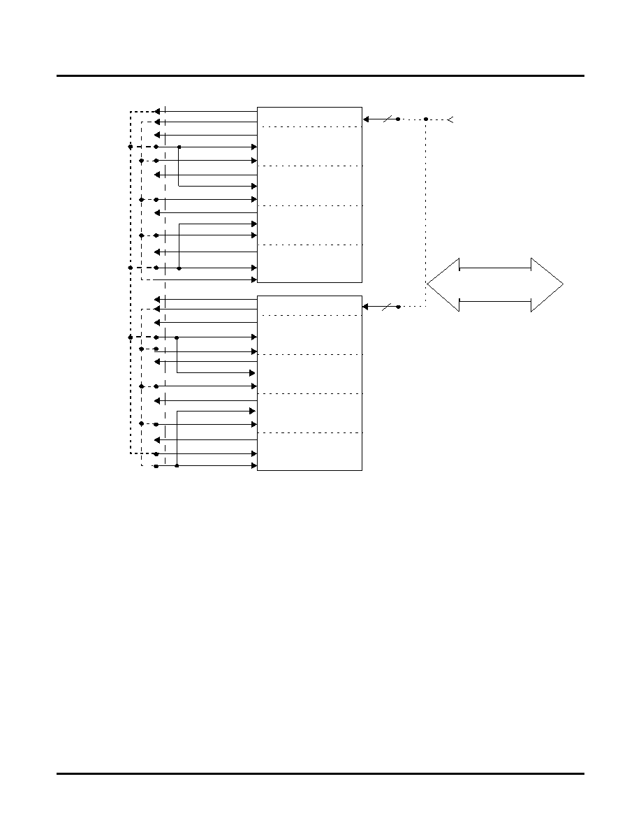
Figure 31. Clocking for Eight Channel Alignment
Reset Operation
The SERDES block can be reset in one of three different ways as follows: on power up, using the hardware reset,
or via the microprocessor interface. The power up reset process begins when the power supply voltage ramps up to
approximately 80% of the nominal value of 1.5V. Following this event, the device will be ready for normal operation
after 3 ms.
A hardware reset is initiated by making the PASB_RESETN low for at least two microprocessor clock cycles. The
device will be ready for operation 3 ms after the low to high transition of the PASB_RESETN. This reset function
affects all SERDES channels and resets all microprocessor and internal registers and counters.
Using the software reset option, each channel can be individually reset by setting SWRST (bit 2) to a logic 1 in the
channel conguration register. The device will be ready 3 ms after the SWRST bit is deasserted. Similarly, all four
channels per quad SERDES can be reset by setting the global reset bit GSWRST. The device will be ready for nor-
mal operation 3 ms after the GSWRST bit is deasserted. Note that the software reset option resets only SERDES
internal registers and counters. The microprocessor registers are not affected. It should also be noted that the
embedded block cannot be accessed until after FPGA conguration is complete.
FPGA
Logic
Common Logic, Quad A
Channel AA
Channel AB
Channel AD
Channel AC
Common Logic, Quad B
Channel BA
Channel BB
Channel BD
Channel BC
RCK78A
TCK78A
RSYS_CLK_A1
TSYS_CLK_AA
RWCKAA
RWCKAB
TSYS_CLK_AB
RWCKAC
TSYS_CLK_AC
RSYS_CLK_A2
TSYS_CLK_AD
RWCKAD
RCK78B
TCK78B
RSYS_CLK_B1
TSYS_CLK_BA
RWCKBA
RWCKBB
TSYS_CLK_BB
RSYS_CLK_B2
RWCKBD
RWCKBC
TSYS_CLK_BC
TSYS_CLK_BD
TCK78A
2
REFCLK[P:N]_A
2
REFCLK[P:N]_B
156.25 MHz
All Clocks at
78.125 MHz
Eight Bidirectional
Channels of 3.125
Gbps Serial Data
相关PDF资料 |
PDF描述 |
|---|---|
| ORT82G5-2FN680I | IC TRANCEIVERS FPSC 680FPBGA |
| VI-J4H-IW-F4 | CONVERTER MOD DC/DC 52V 100W |
| VI-J4H-IW-F3 | CONVERTER MOD DC/DC 52V 100W |
| ORT82G5-1FN680C | IC TRANCEIVERS FPSC 680FPBGA |
| ORT82G5-2FN680C | IC TRANCEIVERS FPSC 680FPBGA |
相关代理商/技术参数 |
参数描述 |
|---|---|
| ORT82G5-1FN680I1 | 功能描述:FPGA - 现场可编程门阵列 10368 LUT 372 I/O RoHS:否 制造商:Altera Corporation 系列:Cyclone V E 栅极数量: 逻辑块数量:943 内嵌式块RAM - EBR:1956 kbit 输入/输出端数量:128 最大工作频率:800 MHz 工作电源电压:1.1 V 最大工作温度:+ 70 C 安装风格:SMD/SMT 封装 / 箱体:FBGA-256 |
| ORT82G5-2BM680C | 功能描述:FPGA - 现场可编程门阵列 10368 LUT 372 I/O RoHS:否 制造商:Altera Corporation 系列:Cyclone V E 栅极数量: 逻辑块数量:943 内嵌式块RAM - EBR:1956 kbit 输入/输出端数量:128 最大工作频率:800 MHz 工作电源电压:1.1 V 最大工作温度:+ 70 C 安装风格:SMD/SMT 封装 / 箱体:FBGA-256 |
| ORT82G5-2BM680I | 功能描述:FPGA - 现场可编程门阵列 10368 LUT 372 I/O RoHS:否 制造商:Altera Corporation 系列:Cyclone V E 栅极数量: 逻辑块数量:943 内嵌式块RAM - EBR:1956 kbit 输入/输出端数量:128 最大工作频率:800 MHz 工作电源电压:1.1 V 最大工作温度:+ 70 C 安装风格:SMD/SMT 封装 / 箱体:FBGA-256 |
| ORT82G5-2F680C | 功能描述:FPGA - 现场可编程门阵列 ORCA FPSC 2.7Gbits/s BP XCVR 643K RoHS:否 制造商:Altera Corporation 系列:Cyclone V E 栅极数量: 逻辑块数量:943 内嵌式块RAM - EBR:1956 kbit 输入/输出端数量:128 最大工作频率:800 MHz 工作电源电压:1.1 V 最大工作温度:+ 70 C 安装风格:SMD/SMT 封装 / 箱体:FBGA-256 |
| ORT82G5-2F680I | 功能描述:FPGA - 现场可编程门阵列 ORCA FPSC 2.7GBITS/s BP XCVR 643K RoHS:否 制造商:Altera Corporation 系列:Cyclone V E 栅极数量: 逻辑块数量:943 内嵌式块RAM - EBR:1956 kbit 输入/输出端数量:128 最大工作频率:800 MHz 工作电源电压:1.1 V 最大工作温度:+ 70 C 安装风格:SMD/SMT 封装 / 箱体:FBGA-256 |
发布紧急采购,3分钟左右您将得到回复。