- 您现在的位置:买卖IC网 > PDF目录11733 > ORT82G5-1FN680I (Lattice Semiconductor Corporation)IC TRANCEIVERS FPSC 680FPBGA PDF资料下载
参数资料
| 型号: | ORT82G5-1FN680I |
| 厂商: | Lattice Semiconductor Corporation |
| 文件页数: | 80/119页 |
| 文件大小: | 0K |
| 描述: | IC TRANCEIVERS FPSC 680FPBGA |
| 产品变化通告: | Product Discontinuation 01/Aug/2011 |
| 标准包装: | 24 |
| 系列: | * |
第1页第2页第3页第4页第5页第6页第7页第8页第9页第10页第11页第12页第13页第14页第15页第16页第17页第18页第19页第20页第21页第22页第23页第24页第25页第26页第27页第28页第29页第30页第31页第32页第33页第34页第35页第36页第37页第38页第39页第40页第41页第42页第43页第44页第45页第46页第47页第48页第49页第50页第51页第52页第53页第54页第55页第56页第57页第58页第59页第60页第61页第62页第63页第64页第65页第66页第67页第68页第69页第70页第71页第72页第73页第74页第75页第76页第77页第78页第79页当前第80页第81页第82页第83页第84页第85页第86页第87页第88页第89页第90页第91页第92页第93页第94页第95页第96页第97页第98页第99页第100页第101页第102页第103页第104页第105页第106页第107页第108页第109页第110页第111页第112页第113页第114页第115页第116页第117页第118页第119页
Lattice Semiconductor
ORCA ORT42G5 and ORT82G5 Data Sheet
63
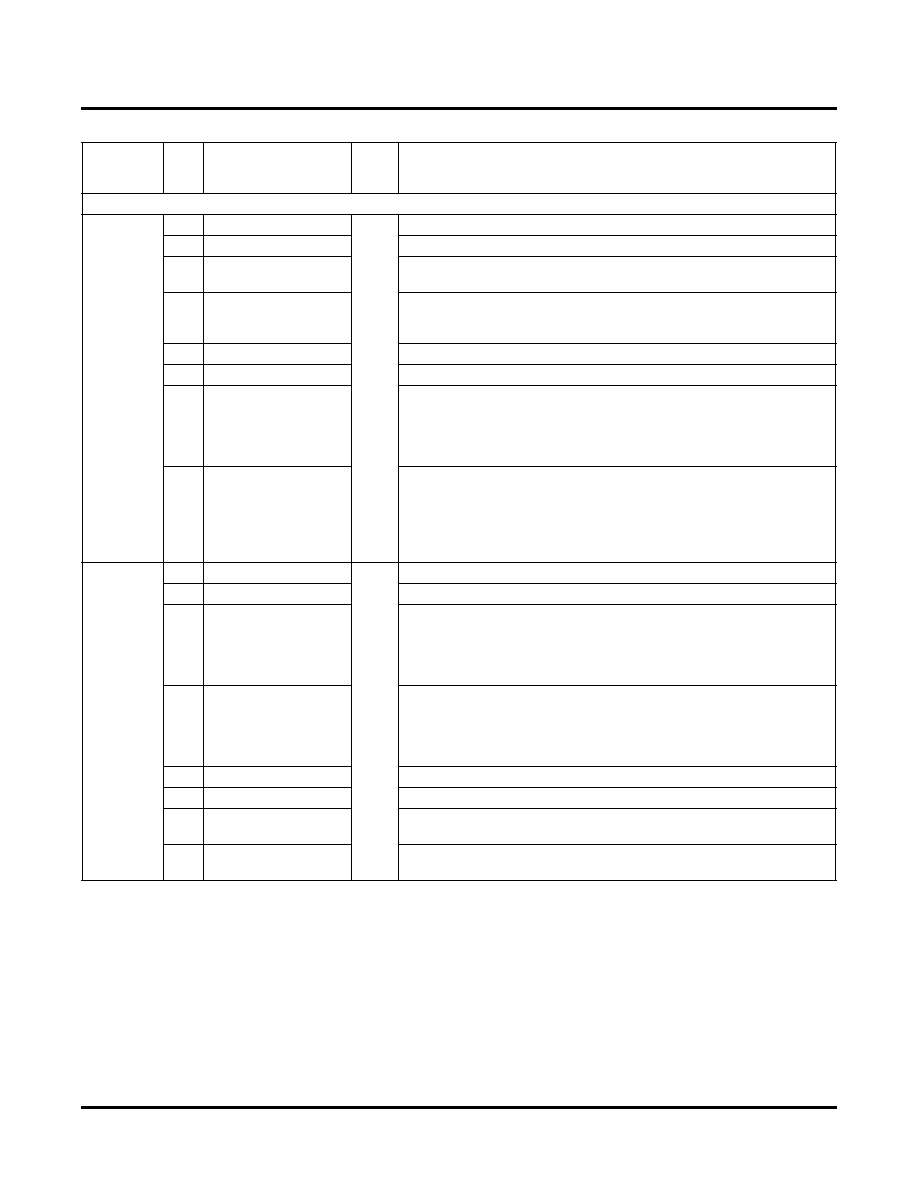
Control Registers (Read/Write), xx=[AC, AD, BC or BD]
30800 - Ax
30900 - Bx
[0]
—
00
Reserved for future use
[1]
—
Reserved for future use
[2]
ENBYSYNC_xC
ENBYSYNC_xC= 1 Enables Receiver Byte Synchronization for Channel
xC. ENBYSYNC_xC = 0 on device reset.
[3]
ENBYSYNC_xD
ENBYSYNC_xD = 1 Enables Receiver Byte Synchronization for Channel
xA. ENBYSYNC_xD = 0 on device reset.
[4]
—
Reserved for future use
[5]
—
Reserved for future use
[6]
LCKREFN_xC
LCKREFN_xC = 0 Locks the receiver PLL to reference clock for Channel
xC.
LCKREFN_xC =1 = Locks the receiver to data for Channel xx.
NOTE: When LCKREFN_xx = 0, the corresponding LKI_xx bit is also 0.
LCKREFN_xC = 0 on device reset.
[7]
LCKREFN_xD
LCKREFN_xD = 0 Locks the receiver PLL to reference clock for Channel
xD.
LCKREFN_xD =1 = Locks the receiver to data for Channel xA.
NOTE: When LCKREFN_xx = 0, the corresponding LKI_xx bit is also 0.
LCKREFN_xD = 0 on device reset.
30801 - Ax
30901 - Bx
[0]
—
00
Reserved for future use
[1]
—
Reserved for future use
[2]
LOOPENB_xC
Enable Loopback Mode for Channel xC. When LOOPEN_xC=1, the
transmitter high-speed output is looped back to the receiver high-speed
input. This mode is similar to high-speed loopback mode enabled by
TESTMODE_xx except that LOOPEN_xx disables the high-speed serial
output. LOOPEN_xC=0 on device reset.
[3]
LOOPENB_xD
Enable Loopback Mode for Channel xD. When LOOPEN_xD=1, the
transmitter high-speed output is looped back to the receiver high-speed
input. This mode is similar to high-speed loopback mode enabled by
TESTMODE_xx except that LOOPEN_xx disables the high-speed serial
output. LOOPEN_xD=0 on device reset.
[4]
—
Reserved for future use
[5]
—
Reserved for future use
[6]
NOWDALIGN_xC
Word Align Disable Bit. When NOWDALIGN_xC=1, receiver word align-
ment is disabled for Channel xC. NOWDALIGN_xC=0 on device reset.
[7]
NOWDALIGN_xD
Word Align Disable Bit. When NOWDALIGN_xD=1, receiver word align-
ment is disabled for Channel xD. NOWDALIGN_xD=0 on device reset.
Table 28. ORT42G5 Memory Map (Continued)
(0x)
Absolute
Address
Bit
Name
Reset
Value
(0x)
Description
相关PDF资料 |
PDF描述 |
|---|---|
| ORT82G5-2FN680I | IC TRANCEIVERS FPSC 680FPBGA |
| VI-J4H-IW-F4 | CONVERTER MOD DC/DC 52V 100W |
| VI-J4H-IW-F3 | CONVERTER MOD DC/DC 52V 100W |
| ORT82G5-1FN680C | IC TRANCEIVERS FPSC 680FPBGA |
| ORT82G5-2FN680C | IC TRANCEIVERS FPSC 680FPBGA |
相关代理商/技术参数 |
参数描述 |
|---|---|
| ORT82G5-1FN680I1 | 功能描述:FPGA - 现场可编程门阵列 10368 LUT 372 I/O RoHS:否 制造商:Altera Corporation 系列:Cyclone V E 栅极数量: 逻辑块数量:943 内嵌式块RAM - EBR:1956 kbit 输入/输出端数量:128 最大工作频率:800 MHz 工作电源电压:1.1 V 最大工作温度:+ 70 C 安装风格:SMD/SMT 封装 / 箱体:FBGA-256 |
| ORT82G5-2BM680C | 功能描述:FPGA - 现场可编程门阵列 10368 LUT 372 I/O RoHS:否 制造商:Altera Corporation 系列:Cyclone V E 栅极数量: 逻辑块数量:943 内嵌式块RAM - EBR:1956 kbit 输入/输出端数量:128 最大工作频率:800 MHz 工作电源电压:1.1 V 最大工作温度:+ 70 C 安装风格:SMD/SMT 封装 / 箱体:FBGA-256 |
| ORT82G5-2BM680I | 功能描述:FPGA - 现场可编程门阵列 10368 LUT 372 I/O RoHS:否 制造商:Altera Corporation 系列:Cyclone V E 栅极数量: 逻辑块数量:943 内嵌式块RAM - EBR:1956 kbit 输入/输出端数量:128 最大工作频率:800 MHz 工作电源电压:1.1 V 最大工作温度:+ 70 C 安装风格:SMD/SMT 封装 / 箱体:FBGA-256 |
| ORT82G5-2F680C | 功能描述:FPGA - 现场可编程门阵列 ORCA FPSC 2.7Gbits/s BP XCVR 643K RoHS:否 制造商:Altera Corporation 系列:Cyclone V E 栅极数量: 逻辑块数量:943 内嵌式块RAM - EBR:1956 kbit 输入/输出端数量:128 最大工作频率:800 MHz 工作电源电压:1.1 V 最大工作温度:+ 70 C 安装风格:SMD/SMT 封装 / 箱体:FBGA-256 |
| ORT82G5-2F680I | 功能描述:FPGA - 现场可编程门阵列 ORCA FPSC 2.7GBITS/s BP XCVR 643K RoHS:否 制造商:Altera Corporation 系列:Cyclone V E 栅极数量: 逻辑块数量:943 内嵌式块RAM - EBR:1956 kbit 输入/输出端数量:128 最大工作频率:800 MHz 工作电源电压:1.1 V 最大工作温度:+ 70 C 安装风格:SMD/SMT 封装 / 箱体:FBGA-256 |
发布紧急采购,3分钟左右您将得到回复。