- 您现在的位置:买卖IC网 > PDF目录11733 > ORT82G5-1FN680I (Lattice Semiconductor Corporation)IC TRANCEIVERS FPSC 680FPBGA PDF资料下载
参数资料
| 型号: | ORT82G5-1FN680I |
| 厂商: | Lattice Semiconductor Corporation |
| 文件页数: | 33/119页 |
| 文件大小: | 0K |
| 描述: | IC TRANCEIVERS FPSC 680FPBGA |
| 产品变化通告: | Product Discontinuation 01/Aug/2011 |
| 标准包装: | 24 |
| 系列: | * |
第1页第2页第3页第4页第5页第6页第7页第8页第9页第10页第11页第12页第13页第14页第15页第16页第17页第18页第19页第20页第21页第22页第23页第24页第25页第26页第27页第28页第29页第30页第31页第32页当前第33页第34页第35页第36页第37页第38页第39页第40页第41页第42页第43页第44页第45页第46页第47页第48页第49页第50页第51页第52页第53页第54页第55页第56页第57页第58页第59页第60页第61页第62页第63页第64页第65页第66页第67页第68页第69页第70页第71页第72页第73页第74页第75页第76页第77页第78页第79页第80页第81页第82页第83页第84页第85页第86页第87页第88页第89页第90页第91页第92页第93页第94页第95页第96页第97页第98页第99页第100页第101页第102页第103页第104页第105页第106页第107页第108页第109页第110页第111页第112页第113页第114页第115页第116页第117页第118页第119页
Lattice Semiconductor
ORCA ORT42G5 and ORT82G5 Data Sheet
20
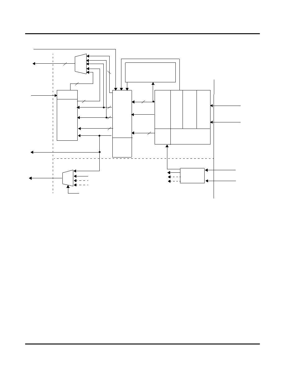
Figure 6. Basic Logic Blocks, Receive Path, Single Channel (Typical Reference Clock Frequency)
Each channel provides its own received clock, received data and K-character detect signals to the FPGA logic.
Incoming data from multiple channels can be aligned using comma (/K/) characters or /A/ character (as specied
either in Fibre Channel specications or in IEEE 802.3ae for XAUI based interfaces). If the 8b/10b decoders are
bypassed, then 40-bit data streams are passed to the FPGA logic. No channel alignment can be done in this
8b/10b bypass mode.
Detailed descriptions of data synchronization, of the SERDES, DEMUX and Multi-Channel Alignment blocks and of
the Fibre Channel and XAUI state machines are given in following sections. Receive clock distribution is described
in a later section of this data sheet.
Synchronization
The SERDES RX logic performs four levels of synchronization on the incoming serial data stream. Each level
builds upon the previous, providing rst bit, then byte (character), then channel (32-bit word), and nally multi-chan-
nel alignment. Each step is described functionally in the following paragraphs. The details of the logical implemen-
tations are described in subsequent sections.
Bit alignment is the task of the Clock/Data Recovery (CDR) block. This block utilizes a PLL that locks to the transi-
tions in the incoming high-speed serial data stream, and outputs the extracted clock as well as the data. If the PLL
is unable to lock to the serial data stream, it instead locks to REFCLK[A:B] to stabilize the voltage-controlled oscil-
lator (VCO), and periodically switches back to the serial data stream to again attempt synchronization. This pro-
cess continues until a valid input data stream is detected and lock is achieved. The CDR can maintain lock on data
as long as the input data stream contains an adequate data “eye” (i.e., jitter is within specication) and the maxi-
mum data stream run length is not exceeded.
REFCLKP_[A:B]
REFCLKN_[A:B]
REFCLK
Buffer
MUX
RCK78[A:B]
78.125 MHz
RCKSEL[0:1][A:B]
Logic Common to Block
From other channel
or channels
To other
channel or
channels
From Control
Register
{
PLL
CML
Buffer
1:10
DEMUX
8B/10B
Encoder
(with
bypass)
HDINP_xx
HDIN_xx
CDR
Byte
Align
RX SERDES Block
XAUI
State
Machine
1:4
DEMUX
(x 10)
156.25 MHz
FIFO
Multi-
Channel
Alignment
FPGA
Logic
Backplane
Serial
Link
RWCKxx
78.125 MHz
Multi-Channel
Alignment Block
78.125 MHz
78.125 MHz Clock
RALIGNxx[3:0]
Align Character Detect
4
RWBIT8xx[3:0]
4 bits k-control
32
RWDxx[31:0]
32-bit data
RSYS_CLK_x#
78.125 MHz
2:1
MUX
(x40)
MRWDxx[39:0]
CV_SELxx
4
RWBIT9xx[3:0]
40
36
32-bit data
4 bits k-ctrl
Synchronization
Status bits
See Table 8
Fibre Channel State
Machine
SRBD_xx[0:9]
DEMUX
Block
SCVxx
312.5 MHz
Clocks
10
2
SBYTSYNC_xx
SWDSYNC_xx
For ORT42G5:
xx = [AC, AD, BC, BD]
x# = [A2, B2]
For ORT82G5:
xx = [AA, AB, ... BD]
x# = [A1, ...B2]
3
FPGA
Logic
相关PDF资料 |
PDF描述 |
|---|---|
| ORT82G5-2FN680I | IC TRANCEIVERS FPSC 680FPBGA |
| VI-J4H-IW-F4 | CONVERTER MOD DC/DC 52V 100W |
| VI-J4H-IW-F3 | CONVERTER MOD DC/DC 52V 100W |
| ORT82G5-1FN680C | IC TRANCEIVERS FPSC 680FPBGA |
| ORT82G5-2FN680C | IC TRANCEIVERS FPSC 680FPBGA |
相关代理商/技术参数 |
参数描述 |
|---|---|
| ORT82G5-1FN680I1 | 功能描述:FPGA - 现场可编程门阵列 10368 LUT 372 I/O RoHS:否 制造商:Altera Corporation 系列:Cyclone V E 栅极数量: 逻辑块数量:943 内嵌式块RAM - EBR:1956 kbit 输入/输出端数量:128 最大工作频率:800 MHz 工作电源电压:1.1 V 最大工作温度:+ 70 C 安装风格:SMD/SMT 封装 / 箱体:FBGA-256 |
| ORT82G5-2BM680C | 功能描述:FPGA - 现场可编程门阵列 10368 LUT 372 I/O RoHS:否 制造商:Altera Corporation 系列:Cyclone V E 栅极数量: 逻辑块数量:943 内嵌式块RAM - EBR:1956 kbit 输入/输出端数量:128 最大工作频率:800 MHz 工作电源电压:1.1 V 最大工作温度:+ 70 C 安装风格:SMD/SMT 封装 / 箱体:FBGA-256 |
| ORT82G5-2BM680I | 功能描述:FPGA - 现场可编程门阵列 10368 LUT 372 I/O RoHS:否 制造商:Altera Corporation 系列:Cyclone V E 栅极数量: 逻辑块数量:943 内嵌式块RAM - EBR:1956 kbit 输入/输出端数量:128 最大工作频率:800 MHz 工作电源电压:1.1 V 最大工作温度:+ 70 C 安装风格:SMD/SMT 封装 / 箱体:FBGA-256 |
| ORT82G5-2F680C | 功能描述:FPGA - 现场可编程门阵列 ORCA FPSC 2.7Gbits/s BP XCVR 643K RoHS:否 制造商:Altera Corporation 系列:Cyclone V E 栅极数量: 逻辑块数量:943 内嵌式块RAM - EBR:1956 kbit 输入/输出端数量:128 最大工作频率:800 MHz 工作电源电压:1.1 V 最大工作温度:+ 70 C 安装风格:SMD/SMT 封装 / 箱体:FBGA-256 |
| ORT82G5-2F680I | 功能描述:FPGA - 现场可编程门阵列 ORCA FPSC 2.7GBITS/s BP XCVR 643K RoHS:否 制造商:Altera Corporation 系列:Cyclone V E 栅极数量: 逻辑块数量:943 内嵌式块RAM - EBR:1956 kbit 输入/输出端数量:128 最大工作频率:800 MHz 工作电源电压:1.1 V 最大工作温度:+ 70 C 安装风格:SMD/SMT 封装 / 箱体:FBGA-256 |
发布紧急采购,3分钟左右您将得到回复。