- 您现在的位置:买卖IC网 > PDF目录299768 > PF38F1020WYTQ1 (INTEL CORP) SPECIALTY MEMORY CIRCUIT, PBGA88 PDF资料下载
参数资料
| 型号: | PF38F1020WYTQ1 |
| 厂商: | INTEL CORP |
| 元件分类: | 存储器 |
| 英文描述: | SPECIALTY MEMORY CIRCUIT, PBGA88 |
| 封装: | 8 X 10 MM, 1.20 MM HEIGHT, 0.80 MM PITCH, LEAD FREE, SCSP-88 |
| 文件页数: | 23/23页 |
| 文件大小: | 364K |
| 代理商: | PF38F1020WYTQ1 |
32-Mbit W18 + 8-Mbit SRAM (38F1020W0YTQ1, 38F1020W0YBQ1)
Datasheet
Intel StrataFlash Wireless Memory (W18 SCSP)
28 Jun 2005
Order Number: 252635, Revision: 003
9
4.1
Signal Descriptions
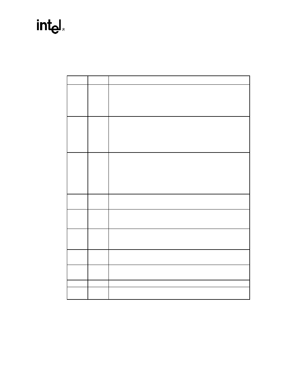
Table 1 describes the active signals used on the 38F1020W0YQ1 devices.
Table 1.
Signal Descriptions (Sheet 1 of 2)
Symbol
Type
Name and Function
A[25:0]
Input
ADDRESS INPUTS: Decodes a specific location for reads or writes, or targets a
flash device block for erase. Flash memory addresses are latched during writes, and
for reads when ADV# (or CLK with ADV# low) is issued.
A[20:0] decodes a specific location within the 28F320W18 die.
A[18:0] decodes a specific location within the 8-Mbit SRAM.
A[25:21] is not used in this SCSP device and is Reserved for Future Use (RFU).
D[15:0]
Input/
Output
DATA INPUTS/OUTPUTS: Inputs data for SRAM writes or flash device
programming. Flash memory commands issued during CUI writes are input on
D[7:0] only.
D[15:0] outputs the device memory contents or flash device ID codes. D[15:0]
are floated when the device is deselected or the outputs are disabled.
Flash memory SRD is read on D[7:0] only.
Flash device I/Os D[15:8, 6:0] are floated when the flash device WSM is busy.
CE#1,
CE#2
Input
FLASH CHIP ENABLE:
CE#1-low selects the flash device.
–
When asserted, the flash device internal control logic, input buffers, decoders,
and
sense amplifiers are activated.
–
When deasserted, the flash die is deselected, power levels reduce to
standby, and data and WAIT outputs are placed in high-Z state.
CE#2 is not used in this SCSP device and is RFU.
S-CS1#,
S-CS2
Input
SRAM CHIP SELECTS: Activates the SRAM internal control logic, input buffers,
decoders, and sense amplifiers. When either are deasserted (S-CS1# = VIH or
S-CS2 = VIL), the SRAM is deselected and its power reduces to standby levels.
RST#
Input
FLASH RESET: RST#-low resets the flash device internal circuitry and inhibits write
operations. Use this function to protect data during power transitions. After exiting
the reset state (RST# returned to logic-high), the selected flash die resumes
operation in asynchronous read-array mode.
OE#1,
OE#2
Input
FLASH OUTPUT ENABLE: OE#1-low activates device output through the flash
memory device data buffers during a flash memory read cycle. When deasserted,
the flash device outputs tristate to high-Z.
OE#2 is not used in this SCSP device and is RFU.
R-OE#
Input
SRAM OUTPUT ENABLE: R-OE#-low activates device output through the SRAM
data buffers during a SRAM read cycle. When deasserted, the SRAM outputs tristate
to high-Z.
WE#
Input
FLASH WRITE ENABLE: WE# controls writes to the selected flash memory die.
WE#-low allows input to the flash device CUI, array, PR/PLR, RCR, or block lock
bits. Addresses and data latch on the signal rising edge.
R-WE#
Input
SRAM WRITE ENABLE: R-WE#-low allows writes to the SRAM array.
R-UB#,
R-LB#
Input
SRAM UPPER / LOWER BYTE ENABLES: R-UB#-low enables the SRAM
high-order bytes (D[15:8]). R-LB#-low enables the SRAM low-order bytes (D[7:0]).
相关PDF资料 |
PDF描述 |
|---|---|
| PF38F3352LLZDQ0 | SPECIALTY MEMORY CIRCUIT, PBGA88 |
| PF38F40L0YUQ0 | 16M X 16 FLASH 1.8V PROM, PBGA88 |
| PF50WIW2K-3.5VF-W6 | SINGLE COLOR LED, INCAND WHITE |
| PD50WO3K-28V-T | SINGLE COLOR LED, SUPER ORANGE |
| PD50WR3K-24V-W6 | SINGLE COLOR LED, ULTRA RED |
相关代理商/技术参数 |
参数描述 |
|---|---|
| PF38F1030W0YBQFA | 制造商:Micron Technology Inc 功能描述:32X/16PS SCSP 1.8 LF WINBOND - Trays |
| PF38F1030W0YBQFB | 制造商:Micron Technology Inc 功能描述:32X/16PS SCSP 1.8 LF WINBOND - Tape and Reel |
| PF38F1030W0YCQEA | 制造商:Micron Technology Inc 功能描述:32X/16PS SCSP 1.8 LF - Trays |
| PF38F1030W0YTQFA | 制造商:Micron Technology Inc 功能描述:32X/16PS SCSP 1.8 LF WINBOND - Trays |
| PF38F1030W0YTQFB | 制造商:Micron Technology Inc 功能描述:32X/16PS SCSP 1.8 LF WINBOND - Tape and Reel |
发布紧急采购,3分钟左右您将得到回复。