- 您现在的位置:买卖IC网 > PDF目录367933 > PH28F128L18T85 (INTEL CORP) StrataFlash Wireless Memory PDF资料下载
参数资料
| 型号: | PH28F128L18T85 |
| 厂商: | INTEL CORP |
| 元件分类: | PROM |
| 英文描述: | StrataFlash Wireless Memory |
| 中文描述: | 8M X 16 FLASH 1.8V PROM, 85 ns, PBGA56 |
| 封装: | 0.75 MM PITCH, LEAD FREE, VFBGA-56 |
| 文件页数: | 49/106页 |
| 文件大小: | 1272K |
| 代理商: | PH28F128L18T85 |
第1页第2页第3页第4页第5页第6页第7页第8页第9页第10页第11页第12页第13页第14页第15页第16页第17页第18页第19页第20页第21页第22页第23页第24页第25页第26页第27页第28页第29页第30页第31页第32页第33页第34页第35页第36页第37页第38页第39页第40页第41页第42页第43页第44页第45页第46页第47页第48页当前第49页第50页第51页第52页第53页第54页第55页第56页第57页第58页第59页第60页第61页第62页第63页第64页第65页第66页第67页第68页第69页第70页第71页第72页第73页第74页第75页第76页第77页第78页第79页第80页第81页第82页第83页第84页第85页第86页第87页第88页第89页第90页第91页第92页第93页第94页第95页第96页第97页第98页第99页第100页第101页第102页第103页第104页第105页第106页
Intel StrataFlash Wireless Memory (L18)
Datasheet
Intel StrataFlash Wireless Memory (L18)
Order Number: 251902, Revision: 009
April 2005
49
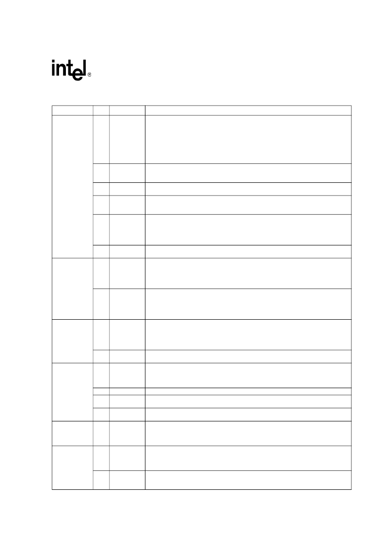
Write
0x40Setup
First cycle of a 2-cycle programming command; prepares the CUI for a write operation.
On the next write cycle, the address and data are latched and the WSM executes the
programming algorithm at the addressed location. During program operations, the
partition responds only to Read Status Register and Program Suspend commands. CE#
or OE# must be toggled to update the Status Register in asynchronous read. CE# or
ADV# must be toggled to update the Status Register Data for synchronous Non-array
read. The Read Array command must be issued to read array data after programming has
finished.
0x10
Alternate Word
Program
Setup
0xE8Program
Buffered
Program
Confirm
Buffered
Enhanced
Factory
Programming
Setup
0xD0Confirm
Equivalent to the Word Program Setup command, 0x40.
This command loads a variable number of bytes up to the buffer size of 32 words onto the
program buffer.
The confirm command is Issued after the data streaming for writing into the buffer is done.
This instructs the WSM to perform the Buffered Program algorithm, writing the data from
the buffer to the flash memory array.
0xD0
0x80
First cycle of a 2-cycle command; initiates Buffered Enhanced Factory Program mode
(Buffered EFP). The CUI then waits for the Buffered EFP Confirm command, 0xD0, that
initiates the Buffered EFP algorithm. All other commands are ignored when Buffered EFP
mode begins.
If the previous command was Buffered EFP Setup (0x80), the CUI latches the address
and data, and prepares the device for Buffered EFP mode.
First cycle of a 2-cycle command; prepares the CUI for a block-erase operation. The
WSM performs the erase algorithm on the block addressed by the Erase Confirm
command. If the next command
is not
the Erase Confirm (0xD0) command, the CUI sets
Status Register bits SR[4] and SR[5], and places the addressed partition in read status
register mode.
If the first command was Block Erase Setup (0x20), the CUI latches the address and data,
and the WSM erases the addressed block. During block-erase operations, the partition
responds only to Read Status Register and Erase Suspend commands. CE# or OE# must
be toggled to update the Status Register in asynchronous read. CE# or ADV# must be
toggled to update the Status Register Data for synchronous Non-array read.
This command issued to any device address initiates a suspend of the currently-
executing program or block erase operation. The Status Register indicates successful
suspend operation by setting either SR[2] (program suspended) or SR[6] (erase
suspended), along with SR[7] (ready). The Write State Machine remains in the suspend
mode regardless of control signal states (except for RST# asserted).
This command issued to any device address resumes the suspended program or block-
erase operation.
First cycle of a 2-cycle command; prepares the CUI for block lock configuration changes.
If the next command is not Block Lock (0x01), Block Unlock (0xD0), or Block Lock-Down
(0x2F), the CUI sets Status Register bits SR[4] and SR[5], indicating a command
sequence error.
If the previous command was Block Lock Setup (0x60), the addressed block is locked.
If the previous command was Block Lock Setup (0x60), the addressed block is unlocked.
If the addressed block is in a lock-down state, the operation has no effect.
If the previous command was Block Lock Setup (0x60), the addressed block is locked
down.
Erase
0x20Setup
0xD0Confirm
Suspend
0xB0
Program or
Erase
Suspend
0xD0Resume
Block Locking/
Unlocking
0x60Setup
0x01 Lock Block
0xD0 Unlock Block
0x2FBlock
Program
Protection
Register
Setup
Read
Configuration
Register
Setup
Read
Configuration
Register
Protection
0xC0
First cycle of a 2-cycle command; prepares the device for a Protection Register or Lock
Register program operation. The second cycle latches the register address and data, and
starts the programming algorithm.
Configuration
0x60
First cycle of a 2-cycle command; prepares the CUI for device read configuration. If the
Set Read Configuration Register command (0x03) is not the next command, the CUI sets
Status Register bits SR[4] and SR[5], indicating a command sequence error.
0x03
If the previous command was Read Configuration Register Setup (0x60), the CUI latches
the address and writes A[15:0] to the Read Configuration Register. Following a Configure
Read Configuration Register command, subsequent read operations access array data.
Table 9.
Command Codes and Definitions (Sheet 2 of 2)
Mode
Code Device Mode
Description
相关PDF资料 |
PDF描述 |
|---|---|
| PH28F256L18B85 | StrataFlash Wireless Memory |
| PH28F256L18T85 | StrataFlash Wireless Memory |
| PH28F640L18B85 | StrataFlash Wireless Memory |
| PH28F640L18T85 | StrataFlash Wireless Memory |
| PH2907A | PNP switching transistor |
相关代理商/技术参数 |
参数描述 |
|---|---|
| PH28F128W18BD60A | 制造商:Micron Technology Inc 功能描述:NOR Flash Parallel 1.8V 128Mbit 8M x 16bit 60ns 56-Pin VFBGA Tray |
| PH28F160C3BD70A | 制造商:Micron Technology Inc 功能描述:MM#865392FLASH 28F160C3BD 70 VF-PBGA46 C |
| PH28F256L18B85 | 制造商:INTEL 制造商全称:Intel Corporation 功能描述:StrataFlash Wireless Memory |
| PH28F256L18B85A | 制造商:Micron Technology Inc 功能描述:MM#875138FLASH 28F256L18B 85 VF-PBGA79 S |
| PH28F256L18T85 | 制造商:INTEL 制造商全称:Intel Corporation 功能描述:StrataFlash Wireless Memory |
发布紧急采购,3分钟左右您将得到回复。