- 您现在的位置:买卖IC网 > PDF目录11546 > PIC12F683-E/MD (Microchip Technology)IC PIC MCU FLASH 2KX14 8DFN PDF资料下载
参数资料
| 型号: | PIC12F683-E/MD |
| 厂商: | Microchip Technology |
| 文件页数: | 105/176页 |
| 文件大小: | 0K |
| 描述: | IC PIC MCU FLASH 2KX14 8DFN |
| 产品培训模块: | Asynchronous Stimulus |
| Digi-Key 应用说明: | AN0005 PWM Example with Microchip's CCP Module AN0005 Example Code |
| 标准包装: | 91 |
| 系列: | PIC® 12F |
| 核心处理器: | PIC |
| 芯体尺寸: | 8-位 |
| 速度: | 20MHz |
| 外围设备: | 欠压检测/复位,POR,PWM,WDT |
| 输入/输出数: | 5 |
| 程序存储器容量: | 3.5KB(2K x 14) |
| 程序存储器类型: | 闪存 |
| EEPROM 大小: | 256 x 8 |
| RAM 容量: | 128 x 8 |
| 电压 - 电源 (Vcc/Vdd): | 2 V ~ 5.5 V |
| 数据转换器: | A/D 4x10b |
| 振荡器型: | 内部 |
| 工作温度: | -40°C ~ 125°C |
| 封装/外壳: | 8-VDFN 裸露焊盘 |
| 包装: | 管件 |
| 配用: | AC164326-ND - MODULA SKT PM3 20QFN I3-DB12F683-ND - BOARD DAUGHTER ICEPIC3 |
第1页第2页第3页第4页第5页第6页第7页第8页第9页第10页第11页第12页第13页第14页第15页第16页第17页第18页第19页第20页第21页第22页第23页第24页第25页第26页第27页第28页第29页第30页第31页第32页第33页第34页第35页第36页第37页第38页第39页第40页第41页第42页第43页第44页第45页第46页第47页第48页第49页第50页第51页第52页第53页第54页第55页第56页第57页第58页第59页第60页第61页第62页第63页第64页第65页第66页第67页第68页第69页第70页第71页第72页第73页第74页第75页第76页第77页第78页第79页第80页第81页第82页第83页第84页第85页第86页第87页第88页第89页第90页第91页第92页第93页第94页第95页第96页第97页第98页第99页第100页第101页第102页第103页第104页当前第105页第106页第107页第108页第109页第110页第111页第112页第113页第114页第115页第116页第117页第118页第119页第120页第121页第122页第123页第124页第125页第126页第127页第128页第129页第130页第131页第132页第133页第134页第135页第136页第137页第138页第139页第140页第141页第142页第143页第144页第145页第146页第147页第148页第149页第150页第151页第152页第153页第154页第155页第156页第157页第158页第159页第160页第161页第162页第163页第164页第165页第166页第167页第168页第169页第170页第171页第172页第173页第174页第175页第176页
PIC12F683
DS41211D-page 32
2007 Microchip Technology Inc.
4.2
Additional Pin Functions
Every
GPIO
pin
on
the
PIC12F683
has
an
interrupt-on-change option and a weak pull-up option.
GP0 has an Ultra Low-Power Wake-up option. The
next three sections describe these functions.
4.2.1
ANSEL REGISTER
The ANSEL register is used to configure the Input
mode of an I/O pin to analog. Setting the appropriate
ANSEL bit high will cause all digital reads on the pin to
be read as ‘0’ and allow analog functions on the pin to
operate correctly.
The state of the ANSEL bits has no affect on digital
output functions. A pin with TRIS clear and ANSEL set
will still operate as a digital output, but the Input mode
will be analog. This can cause unexpected behavior
when executing read-modify-write instructions on the
affected port.
4.2.2
WEAK PULL-UPS
Each of the GPIO pins, except GP3, has an individually
configurable internal weak pull-up. Control bits WPUx
enable or disable each pull-up. Refer to Register 4-4.
Each weak pull-up is automatically turned off when the
port pin is configured as an output. The pull-ups are
disabled on a Power-on Reset by the GPPU bit of the
OPTION register). A weak pull-up is automatically
enabled for GP3 when configured as MCLR and
disabled when GP3 is an I/O. There is no software
control of the MCLR pull-up.
4.2.3
INTERRUPT-ON-CHANGE
Each of the GPIO pins is individually configurable as an
interrupt-on-change pin. Control bits IOCx enable or
disable the interrupt function for each pin. Refer to
Register 4-5. The interrupt-on-change is disabled on a
Power-on Reset.
For enabled interrupt-on-change pins, the values are
compared with the old value latched on the last read of
GPIO. The ‘mismatch’ outputs of the last read are OR’d
together to set the GPIO Change Interrupt Flag bit
(GPIF) in the INTCON register (Register 3-3).
This interrupt can wake the device from Sleep. The
user, in the Interrupt Service Routine, clears the
interrupt by:
a)
Any read or write of GPIO. This will end the
mismatch condition, then,
b)
Clear the flag bit GPIF.
A mismatch condition will continue to set flag bit GPIF.
Reading GPIO will end the mismatch condition and
allow flag bit GPIF to be cleared. The latch holding the
last read value is not affected by a MCLR nor
Brown-out Reset. After these resets, the GPIF flag will
continue to be set if a mismatch is present.
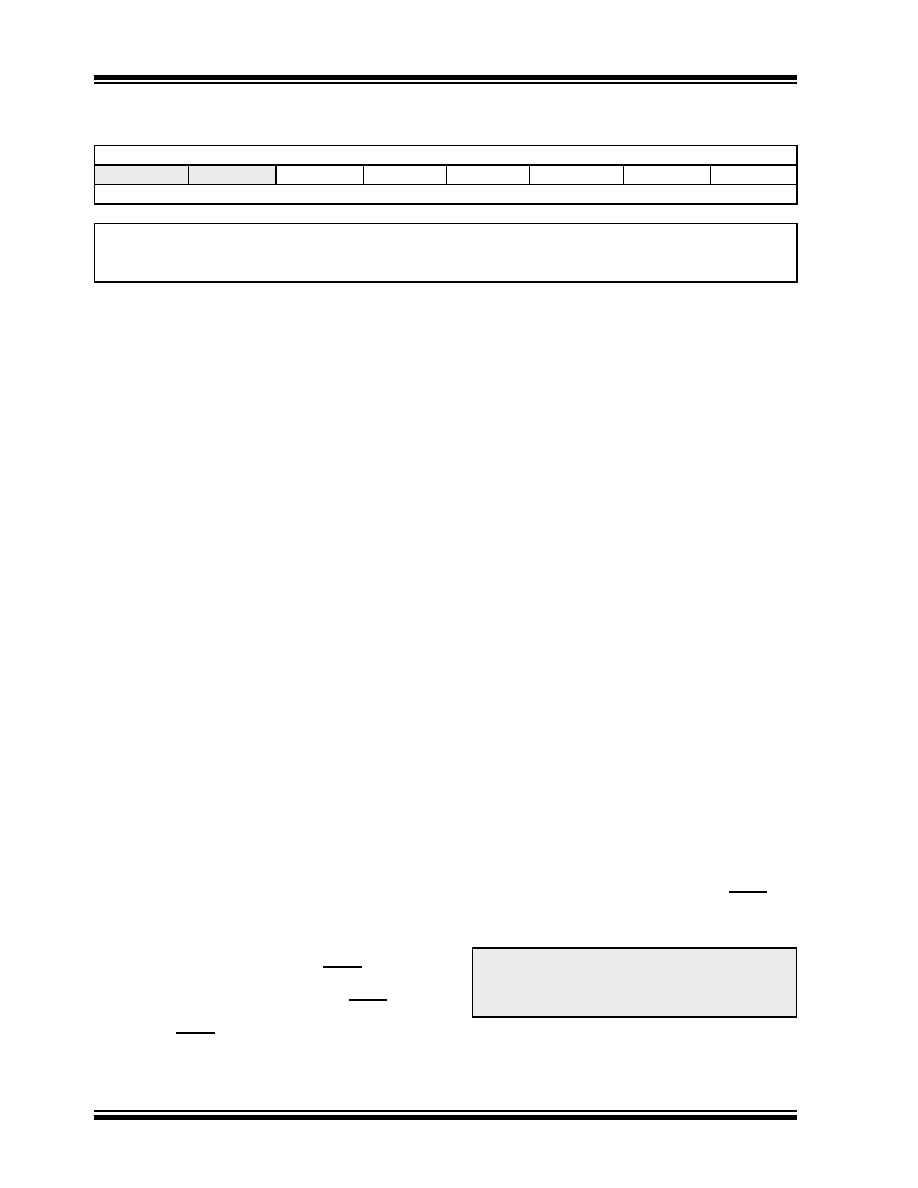
REGISTER 4-2:
TRISIO GPIO TRI-STATE REGISTER
U-0
R/W-1
R-1
R/W-1
—
—TRISIO5(2,3)
TRISIO4(2)
TRISIO3(1)
TRISIO2
TRISIO1
TRISIO0
bit 7
bit 0
Legend:
R = Readable bit
W = Writable bit
U = Unimplemented bit, read as ‘0’
-n = Value at POR
‘1’ = Bit is set
‘0’ = Bit is cleared
x = Bit is unknown
bit 7-6
Unimplemented: Read as ‘0’
bit 5:4
TRISIO<5:4>: GPIO Tri-State Control bit
1
= GPIO pin configured as an input (tri-stated)
0
= GPIO pin configured as an output
bit 3
TRISIO<3>: GPIO Tri-State Control bit
Input only
bit 2:0
TRISIO<2:0>: GPIO Tri-State Control bit
1
= GPIO pin configured as an input (tri-stated)
0
= GPIO pin configured as an output
Note
1:
TRISIO<3> always reads ‘1’.
2:
TRISIO<5:4> always reads ‘1’ in XT, HS and LP OSC modes.
3:
TRISIO<5> always reads ‘1’ in RC and RCIO and EC modes.
Note:
If a change on the I/O pin should occur
when
any
GPIO
operation
is
being
executed, then the GPIF interrupt flag may
not get set.
相关PDF资料 |
PDF描述 |
|---|---|
| PIC18LF43K22T-I/MV | IC MCU 8BIT 8KB FLASH 40UQFN |
| V375C48M75BG | CONVERTER MOD DC/DC 48V 75W |
| V375C48M75BF | CONVERTER MOD DC/DC 48V 75W |
| PIC18F43K22T-I/MV | IC MCU 8BIT 8KB FLASH 40UQFN |
| V375C48M75B3 | CONVERTER MOD DC/DC 48V 75W |
相关代理商/技术参数 |
参数描述 |
|---|---|
| PIC12F683-I/MD | 功能描述:8位微控制器 -MCU 3.5KB 128 RAM 6I/O RoHS:否 制造商:Silicon Labs 核心:8051 处理器系列:C8051F39x 数据总线宽度:8 bit 最大时钟频率:50 MHz 程序存储器大小:16 KB 数据 RAM 大小:1 KB 片上 ADC:Yes 工作电源电压:1.8 V to 3.6 V 工作温度范围:- 40 C to + 105 C 封装 / 箱体:QFN-20 安装风格:SMD/SMT |
| PIC12F683-I/MDQTP | 制造商:MICROCHIP 制造商全称:Microchip Technology 功能描述:8-Pin Flash-Based, 8-Bit CMOS Microcontrollers with nanoWatt Technology |
| PIC12F683-I/MF | 功能描述:8位微控制器 -MCU 3.5KB 128 RAM 6 I/O RoHS:否 制造商:Silicon Labs 核心:8051 处理器系列:C8051F39x 数据总线宽度:8 bit 最大时钟频率:50 MHz 程序存储器大小:16 KB 数据 RAM 大小:1 KB 片上 ADC:Yes 工作电源电压:1.8 V to 3.6 V 工作温度范围:- 40 C to + 105 C 封装 / 箱体:QFN-20 安装风格:SMD/SMT |
| PIC12F683-I/MF | 制造商:Microchip Technology Inc 功能描述:8BIT FLASH MCU SMD 12F683 DFN-8 |
| PIC12F683-I/MFQTP | 制造商:MICROCHIP 制造商全称:Microchip Technology 功能描述:8-Pin Flash-Based, 8-Bit CMOS Microcontrollers with nanoWatt Technology |
发布紧急采购,3分钟左右您将得到回复。