- 您现在的位置:买卖IC网 > PDF目录11310 > PIC18F252-E/SO (Microchip Technology)IC MCU CMOS 40MHZ 16K FLSH28SOIC PDF资料下载
参数资料
| 型号: | PIC18F252-E/SO |
| 厂商: | Microchip Technology |
| 文件页数: | 117/134页 |
| 文件大小: | 0K |
| 描述: | IC MCU CMOS 40MHZ 16K FLSH28SOIC |
| 产品培训模块: | Asynchronous Stimulus |
| 标准包装: | 27 |
| 系列: | PIC® 18F |
| 核心处理器: | PIC |
| 芯体尺寸: | 8-位 |
| 速度: | 40MHz |
| 连通性: | I²C,SPI,UART/USART |
| 外围设备: | 欠压检测/复位,LVD,POR,PWM,WDT |
| 输入/输出数: | 23 |
| 程序存储器容量: | 32KB(16K x 16) |
| 程序存储器类型: | 闪存 |
| EEPROM 大小: | 256 x 8 |
| RAM 容量: | 1.5K x 8 |
| 电压 - 电源 (Vcc/Vdd): | 4.2 V ~ 5.5 V |
| 数据转换器: | A/D 5x10b |
| 振荡器型: | 外部 |
| 工作温度: | -40°C ~ 125°C |
| 封装/外壳: | 28-SOIC(0.295",7.50mm 宽) |
| 包装: | 管件 |
第1页第2页第3页第4页第5页第6页第7页第8页第9页第10页第11页第12页第13页第14页第15页第16页第17页第18页第19页第20页第21页第22页第23页第24页第25页第26页第27页第28页第29页第30页第31页第32页第33页第34页第35页第36页第37页第38页第39页第40页第41页第42页第43页第44页第45页第46页第47页第48页第49页第50页第51页第52页第53页第54页第55页第56页第57页第58页第59页第60页第61页第62页第63页第64页第65页第66页第67页第68页第69页第70页第71页第72页第73页第74页第75页第76页第77页第78页第79页第80页第81页第82页第83页第84页第85页第86页第87页第88页第89页第90页第91页第92页第93页第94页第95页第96页第97页第98页第99页第100页第101页第102页第103页第104页第105页第106页第107页第108页第109页第110页第111页第112页第113页第114页第115页第116页当前第117页第118页第119页第120页第121页第122页第123页第124页第125页第126页第127页第128页第129页第130页第131页第132页第133页第134页
1997 Microchip Technology Inc.
DS30444E - page 83
PIC16C9XX
12.2
Selecting the A/D Conversion Clock
The A/D conversion time per bit is dened as TAD. The
A/D conversion requires 9.5 TAD per 8-bit conversion.
The source of the A/D conversion clock is software
selected. The four possible options for TAD are:
2TOSC
8TOSC
32TOSC
Internal RC oscillator
For correct A/D conversions, the A/D conversion clock
(TAD) must be selected to ensure a minimum TAD time
of 1.6
s.
the device operating frequencies and the A/D clock
source selected.
12.3
Conguring Analog Port Pins
The ADCON1 and TRISA registers control the opera-
tion of the A/D port pins. The port pins that are desired
as analog inputs must have their corresponding TRIS
bits set (input). If the TRIS bit is cleared (output), the
digital output level (VOH or VOL) will be converted.
The A/D operation is independent of the state of the
CHS2:CHS0 bits and the TRIS bits.
Note 1: When reading the port register, all pins
congured as analog inputs will read as
cleared (a low level). Pins congured as
digital inputs, will convert an analog input.
Analog levels on a digitally congured
input will not affect the conversion accu-
racy.
Note 2: Analog levels on any pin that is dened as
a digital input (including the AN4:AN0
pins), may cause the input buffer to con-
sume current that is out of the devices
specication.
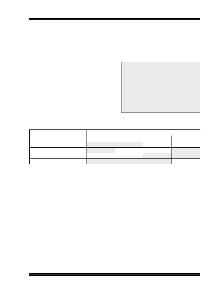
TABLE 12-1: TAD vs. DEVICE OPERATING FREQUENCIES
A/D Clock Source (TAD)
Device Frequency
Operation
ADCS1:ADCS0
8 MHz
5 MHz
1.25 MHz
333.33 kHz
2TOSC
00
250 ns(2)
400 ns(2)
1.6
s
6
s
8TOSC
01
1
s
1.6
s
6.4
s
24
s(3)
32TOSC
10
4
s
6.4
s
25.6
s(3)
96
s(3)
RC
11
2 - 6
s(1,4)
2 - 6
s(1,4)
2 - 6
s(1,4)
2 - 6
s(1)
Legend: Shaded cells are outside of recommended range.
Note 1: The RC source has a typical TAD time of 4
s.
2: These values violate the minimum required TAD time.
3: For faster conversion times, the selection of another clock source is recommended.
4: When derived frequency is greater than 1 MHz, the RC A/D conversion clock source is recommended for
sleep mode only
5: For extended voltage devices (LC), please refer to the electrical specications section.
相关PDF资料 |
PDF描述 |
|---|---|
| VE-24J-IY-S | CONVERTER MOD DC/DC 36V 50W |
| PIC18F4320T-I/PT | IC MCU FLASH 4KX16 EEPROM 44TQFP |
| DSPIC33FJ64MC710A-E/PT | IC DSPIC MCU/DSP 64K 100-TQFP |
| PIC16F876-10E/SP | IC MCU FLASH 8KX14 EE 28DIP |
| PIC16F876-10E/SO | IC MCU FLASH 8KX14 EE 28SOIC |
相关代理商/技术参数 |
参数描述 |
|---|---|
| PIC18F252-I/SO | 功能描述:8位微控制器 -MCU 32KB 1536 RAM 23 I/O RoHS:否 制造商:Silicon Labs 核心:8051 处理器系列:C8051F39x 数据总线宽度:8 bit 最大时钟频率:50 MHz 程序存储器大小:16 KB 数据 RAM 大小:1 KB 片上 ADC:Yes 工作电源电压:1.8 V to 3.6 V 工作温度范围:- 40 C to + 105 C 封装 / 箱体:QFN-20 安装风格:SMD/SMT |
| PIC18F252-I/SO | 制造商:Microchip Technology Inc 功能描述:8BIT FLASH MCU SMD 18F252 SOIC28 |
| PIC18F252-I/SOG | 功能描述:8位微控制器 -MCU 32KB 1536 RAM 23I/O RoHS:否 制造商:Silicon Labs 核心:8051 处理器系列:C8051F39x 数据总线宽度:8 bit 最大时钟频率:50 MHz 程序存储器大小:16 KB 数据 RAM 大小:1 KB 片上 ADC:Yes 工作电源电压:1.8 V to 3.6 V 工作温度范围:- 40 C to + 105 C 封装 / 箱体:QFN-20 安装风格:SMD/SMT |
| PIC18F252-I/SP | 功能描述:8位微控制器 -MCU 32KB 1536 RAM 23I/O RoHS:否 制造商:Silicon Labs 核心:8051 处理器系列:C8051F39x 数据总线宽度:8 bit 最大时钟频率:50 MHz 程序存储器大小:16 KB 数据 RAM 大小:1 KB 片上 ADC:Yes 工作电源电压:1.8 V to 3.6 V 工作温度范围:- 40 C to + 105 C 封装 / 箱体:QFN-20 安装风格:SMD/SMT |
| PIC18F252-I/SP | 制造商:Microchip Technology Inc 功能描述:IC 8BIT FLASH MCU 18F252 SDIL28 |
发布紧急采购,3分钟左右您将得到回复。