- 您现在的位置:买卖IC网 > PDF目录11310 > PIC18F252-E/SO (Microchip Technology)IC MCU CMOS 40MHZ 16K FLSH28SOIC PDF资料下载
参数资料
| 型号: | PIC18F252-E/SO |
| 厂商: | Microchip Technology |
| 文件页数: | 90/134页 |
| 文件大小: | 0K |
| 描述: | IC MCU CMOS 40MHZ 16K FLSH28SOIC |
| 产品培训模块: | Asynchronous Stimulus |
| 标准包装: | 27 |
| 系列: | PIC® 18F |
| 核心处理器: | PIC |
| 芯体尺寸: | 8-位 |
| 速度: | 40MHz |
| 连通性: | I²C,SPI,UART/USART |
| 外围设备: | 欠压检测/复位,LVD,POR,PWM,WDT |
| 输入/输出数: | 23 |
| 程序存储器容量: | 32KB(16K x 16) |
| 程序存储器类型: | 闪存 |
| EEPROM 大小: | 256 x 8 |
| RAM 容量: | 1.5K x 8 |
| 电压 - 电源 (Vcc/Vdd): | 4.2 V ~ 5.5 V |
| 数据转换器: | A/D 5x10b |
| 振荡器型: | 外部 |
| 工作温度: | -40°C ~ 125°C |
| 封装/外壳: | 28-SOIC(0.295",7.50mm 宽) |
| 包装: | 管件 |
第1页第2页第3页第4页第5页第6页第7页第8页第9页第10页第11页第12页第13页第14页第15页第16页第17页第18页第19页第20页第21页第22页第23页第24页第25页第26页第27页第28页第29页第30页第31页第32页第33页第34页第35页第36页第37页第38页第39页第40页第41页第42页第43页第44页第45页第46页第47页第48页第49页第50页第51页第52页第53页第54页第55页第56页第57页第58页第59页第60页第61页第62页第63页第64页第65页第66页第67页第68页第69页第70页第71页第72页第73页第74页第75页第76页第77页第78页第79页第80页第81页第82页第83页第84页第85页第86页第87页第88页第89页当前第90页第91页第92页第93页第94页第95页第96页第97页第98页第99页第100页第101页第102页第103页第104页第105页第106页第107页第108页第109页第110页第111页第112页第113页第114页第115页第116页第117页第118页第119页第120页第121页第122页第123页第124页第125页第126页第127页第128页第129页第130页第131页第132页第133页第134页
1997 Microchip Technology Inc.
DS30444E - page 59
PIC16C9XX
10.2.1
TIMER1 MODE SELECTION
Timer1 must be running in Timer mode or Synchro-
nized Counter mode if the CCP module is using the
compare feature. In Asynchronous Counter mode, the
compare operation may not work.
10.2.2
SOFTWARE INTERRUPT MODE
When Generate Software Interrupt is chosen, the
CCP1 pin is not affected. Only a CCP interrupt is gen-
erated (if enabled).
10.2.3
SPECIAL EVENT TRIGGER
In this mode, an internal hardware trigger is generated
which may be used to initiate an action.
The special event trigger output of CCP1 resets the
TMR1 register pair and starts an A/D conversion. This
allows the CCPR1H:CCPR1L register pair to effectively
be a 16-bit programmable period register for Timer1.
10.3
PWM Mode
In Pulse Width Modulation (PWM) mode, the CCP1 pin
produces up to a 10-bit resolution PWM output. Since
the CCP1 pin is multiplexed with the PORTC data latch,
the TRISC<2> bit must be cleared to make the CCP1
pin an output.
Figure 10-4 shows a simplied block diagram of the
CCP module in PWM mode.
For a step by step procedure on how to set up the CCP
module for PWM operation, see Section 10.3.3.
Note:
The "special event trigger" from the CCP1
module will not set interrupt ag bit
TMR1IF (PIR1<0>).
Note:
Clearing the CCP1CON register will force
the CCP1 PWM output latch to the default
low level. This is not the PORTC I/O data
latch.
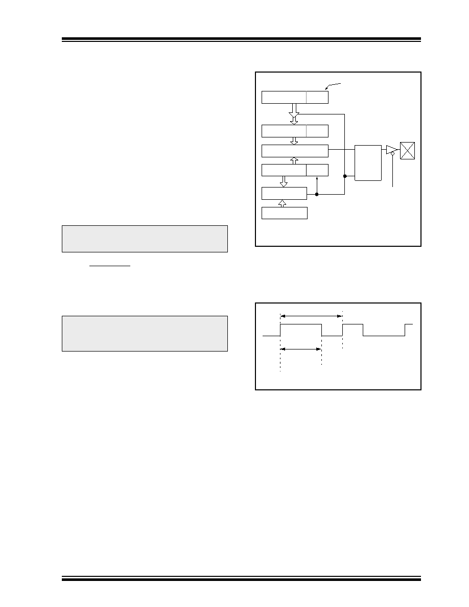
FIGURE 10-4: SIMPLIFIED PWM BLOCK
DIAGRAM
A PWM output (Figure 10-5) has a time-base (period)
and a time that the output stays high (duty cycle). The
frequency of the PWM is the inverse of the period
(1/period).
FIGURE 10-5: PWM OUTPUT
10.3.1
PWM PERIOD
The PWM period is specied by writing to the PR2 reg-
ister. The PWM period can be calculated using the fol-
lowing formula:
PWM period = [ (PR2) + 1 ] 4 TOSC
(TMR2 prescale value)
PWM frequency is dened as 1 / [PWM period].
When TMR2 is equal to PR2, the following three events
occur on the next increment cycle:
TMR2 is cleared
The CCP1 pin is set (exception: if PWM duty
cycle = 0%, the CCP1 pin will not be set)
The PWM duty cycle is latched from CCPR1L into
CCPR1H
CCPR1L
CCPR1H (Slave)
Comparator
TMR2
Comparator
PR2
(Note 1)
R
Q
S
Duty cycle registers
CCP1CON<5:4>
Clear Timer,
CCP1 pin and
latch D.C.
TRISC<2>
RC1/CCP1
Note 1: 8-bit timer is concatenated with 2-bit internal Q clock
or 2 bits of the prescaler to create 10-bit time-base.
Period
Duty Cycle
TMR2 = PR2
TMR2 = Duty Cycle
TMR2 = PR2
相关PDF资料 |
PDF描述 |
|---|---|
| VE-24J-IY-S | CONVERTER MOD DC/DC 36V 50W |
| PIC18F4320T-I/PT | IC MCU FLASH 4KX16 EEPROM 44TQFP |
| DSPIC33FJ64MC710A-E/PT | IC DSPIC MCU/DSP 64K 100-TQFP |
| PIC16F876-10E/SP | IC MCU FLASH 8KX14 EE 28DIP |
| PIC16F876-10E/SO | IC MCU FLASH 8KX14 EE 28SOIC |
相关代理商/技术参数 |
参数描述 |
|---|---|
| PIC18F252-I/SO | 功能描述:8位微控制器 -MCU 32KB 1536 RAM 23 I/O RoHS:否 制造商:Silicon Labs 核心:8051 处理器系列:C8051F39x 数据总线宽度:8 bit 最大时钟频率:50 MHz 程序存储器大小:16 KB 数据 RAM 大小:1 KB 片上 ADC:Yes 工作电源电压:1.8 V to 3.6 V 工作温度范围:- 40 C to + 105 C 封装 / 箱体:QFN-20 安装风格:SMD/SMT |
| PIC18F252-I/SO | 制造商:Microchip Technology Inc 功能描述:8BIT FLASH MCU SMD 18F252 SOIC28 |
| PIC18F252-I/SOG | 功能描述:8位微控制器 -MCU 32KB 1536 RAM 23I/O RoHS:否 制造商:Silicon Labs 核心:8051 处理器系列:C8051F39x 数据总线宽度:8 bit 最大时钟频率:50 MHz 程序存储器大小:16 KB 数据 RAM 大小:1 KB 片上 ADC:Yes 工作电源电压:1.8 V to 3.6 V 工作温度范围:- 40 C to + 105 C 封装 / 箱体:QFN-20 安装风格:SMD/SMT |
| PIC18F252-I/SP | 功能描述:8位微控制器 -MCU 32KB 1536 RAM 23I/O RoHS:否 制造商:Silicon Labs 核心:8051 处理器系列:C8051F39x 数据总线宽度:8 bit 最大时钟频率:50 MHz 程序存储器大小:16 KB 数据 RAM 大小:1 KB 片上 ADC:Yes 工作电源电压:1.8 V to 3.6 V 工作温度范围:- 40 C to + 105 C 封装 / 箱体:QFN-20 安装风格:SMD/SMT |
| PIC18F252-I/SP | 制造商:Microchip Technology Inc 功能描述:IC 8BIT FLASH MCU 18F252 SDIL28 |
发布紧急采购,3分钟左右您将得到回复。