- 您现在的位置:买卖IC网 > PDF目录11310 > PIC18F252-E/SO (Microchip Technology)IC MCU CMOS 40MHZ 16K FLSH28SOIC PDF资料下载
参数资料
| 型号: | PIC18F252-E/SO |
| 厂商: | Microchip Technology |
| 文件页数: | 52/134页 |
| 文件大小: | 0K |
| 描述: | IC MCU CMOS 40MHZ 16K FLSH28SOIC |
| 产品培训模块: | Asynchronous Stimulus |
| 标准包装: | 27 |
| 系列: | PIC® 18F |
| 核心处理器: | PIC |
| 芯体尺寸: | 8-位 |
| 速度: | 40MHz |
| 连通性: | I²C,SPI,UART/USART |
| 外围设备: | 欠压检测/复位,LVD,POR,PWM,WDT |
| 输入/输出数: | 23 |
| 程序存储器容量: | 32KB(16K x 16) |
| 程序存储器类型: | 闪存 |
| EEPROM 大小: | 256 x 8 |
| RAM 容量: | 1.5K x 8 |
| 电压 - 电源 (Vcc/Vdd): | 4.2 V ~ 5.5 V |
| 数据转换器: | A/D 5x10b |
| 振荡器型: | 外部 |
| 工作温度: | -40°C ~ 125°C |
| 封装/外壳: | 28-SOIC(0.295",7.50mm 宽) |
| 包装: | 管件 |
第1页第2页第3页第4页第5页第6页第7页第8页第9页第10页第11页第12页第13页第14页第15页第16页第17页第18页第19页第20页第21页第22页第23页第24页第25页第26页第27页第28页第29页第30页第31页第32页第33页第34页第35页第36页第37页第38页第39页第40页第41页第42页第43页第44页第45页第46页第47页第48页第49页第50页第51页当前第52页第53页第54页第55页第56页第57页第58页第59页第60页第61页第62页第63页第64页第65页第66页第67页第68页第69页第70页第71页第72页第73页第74页第75页第76页第77页第78页第79页第80页第81页第82页第83页第84页第85页第86页第87页第88页第89页第90页第91页第92页第93页第94页第95页第96页第97页第98页第99页第100页第101页第102页第103页第104页第105页第106页第107页第108页第109页第110页第111页第112页第113页第114页第115页第116页第117页第118页第119页第120页第121页第122页第123页第124页第125页第126页第127页第128页第129页第130页第131页第132页第133页第134页
Micrel, Inc.
KSZ8864RMN
April 2012
24
M9999-043012-1.5
On-Chip Termination Resistors
The KSZ8864RMN reduces board cost and simplifies board layout by using on-chip termination resistors for RX/TX
differential pairs without the external termination resistors. The solution of the on chip termination and internal biasing will
enhance much power consumption compare with using external biasing and termination resistors, and the transformer will
not consume power any longer. The center tap doesn’t need to be tied to analog power, just leave them floating or
connect the capacitors to ground separately.
Functional Overview: Power Management
The KSZ8864RMN can also use multiple power level of 3.3V, 2.5V or 1.8V for VDDIO to support different I/O voltage.
The KSZ8864RMN supports enhanced power management feature in low power state with energy detection to ensure
low-power dissipation during device idle periods. There are five operation modes under the power management function
which is controlled by the Register 14 bit [4:3] and the Port Register Control 13 bit3 as shown below:
Register 14 bit [4:3] = 00 Normal Operation Mode
Register 14 bit [4:3] = 01 Energy Detect Mode
Register 14 bit [4:3] = 10 Soft Power Down Mode
Register 14 bit [4:3] = 11 Power Saving Mode
The Port Register Control 13 bit 3 =1 is for the Port Based Power-Down Mode
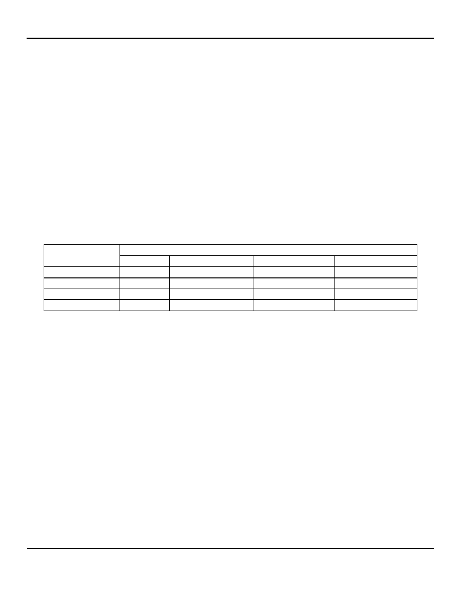
Table 2 indicates all internal function blocks status under four different power management operation modes.
Power Management Operation Modes
KSZ8864RMN
Function Blocks
Normal Mode
Power Saving Mode
Energy Detect Mode
Soft Power Down Mode
Internal PLL Clock
Enabled
Disabled
Tx/Rx PHY
Enabled
Rx unused block disabled
Energy detect at Rx
Disabled
MAC
Enabled
Disabled
Host Interface
Enabled
Disabled
Table 2. Internal Function Block Status
Normal Operation Mode
This is the default setting bit [4:3] =00 in register 14 after the chip power-up or hardware reset. When KSZ8864RMN is in
this normal operation mode, all PLL clocks are running, PHY and MAC are on and the host interface is ready for CPU
read or write.
During the normal operation mode, the host CPU can set the bit [4:3] in register 14 to transit the current normal operation
mode to any one of the other three power management operation modes.
Energy Detect Mode
The energy detect mode provides a mechanism to save more power than in the normal operation mode when the
KSZ8864RMN is not connected to an active link partner. In this mode, if the cable is not plugged, then the KSZ8864RMN
can automatically enter to a low power state, i.e., the energy detect mode. In this mode, KSZ8864RMN will keep
transmitting 120ns width pulses at 1 pulse/s rate. Once activity resumes due to plugging a cable or attempting by the far
end to establish link, the KSZ8864RMN can automatically power up to normal power state in energy detect mode.
Energy detect mode consists of two states, normal power state and low power state. While in low power state, the
KSZ8864RMN reduces power consumption by disabling all circuitry except the energy detect circuitry of the receiver. The
energy detect mode is entered by setting bit [4:3] = 01 in register 14. When the KSZ8864RMN is in this mode, it will
monitor the cable energy. If there is no energy on the cable for a time longer than pre-configured value at bit [7:0] Go-
Sleep time in register 15, then the KSZ8864RMN will go into a low power state. When KSZ8864RMN is in low power
state, it will keep monitoring the cable energy. Once the energy is detected from the cable, KSZ8864RMN will enter
normal power state. When KSZ8864RMN is at normal power state, it is able to transmit or receive packet from the cable.
相关PDF资料 |
PDF描述 |
|---|---|
| VE-24J-IY-S | CONVERTER MOD DC/DC 36V 50W |
| PIC18F4320T-I/PT | IC MCU FLASH 4KX16 EEPROM 44TQFP |
| DSPIC33FJ64MC710A-E/PT | IC DSPIC MCU/DSP 64K 100-TQFP |
| PIC16F876-10E/SP | IC MCU FLASH 8KX14 EE 28DIP |
| PIC16F876-10E/SO | IC MCU FLASH 8KX14 EE 28SOIC |
相关代理商/技术参数 |
参数描述 |
|---|---|
| PIC18F252-I/SO | 功能描述:8位微控制器 -MCU 32KB 1536 RAM 23 I/O RoHS:否 制造商:Silicon Labs 核心:8051 处理器系列:C8051F39x 数据总线宽度:8 bit 最大时钟频率:50 MHz 程序存储器大小:16 KB 数据 RAM 大小:1 KB 片上 ADC:Yes 工作电源电压:1.8 V to 3.6 V 工作温度范围:- 40 C to + 105 C 封装 / 箱体:QFN-20 安装风格:SMD/SMT |
| PIC18F252-I/SO | 制造商:Microchip Technology Inc 功能描述:8BIT FLASH MCU SMD 18F252 SOIC28 |
| PIC18F252-I/SOG | 功能描述:8位微控制器 -MCU 32KB 1536 RAM 23I/O RoHS:否 制造商:Silicon Labs 核心:8051 处理器系列:C8051F39x 数据总线宽度:8 bit 最大时钟频率:50 MHz 程序存储器大小:16 KB 数据 RAM 大小:1 KB 片上 ADC:Yes 工作电源电压:1.8 V to 3.6 V 工作温度范围:- 40 C to + 105 C 封装 / 箱体:QFN-20 安装风格:SMD/SMT |
| PIC18F252-I/SP | 功能描述:8位微控制器 -MCU 32KB 1536 RAM 23I/O RoHS:否 制造商:Silicon Labs 核心:8051 处理器系列:C8051F39x 数据总线宽度:8 bit 最大时钟频率:50 MHz 程序存储器大小:16 KB 数据 RAM 大小:1 KB 片上 ADC:Yes 工作电源电压:1.8 V to 3.6 V 工作温度范围:- 40 C to + 105 C 封装 / 箱体:QFN-20 安装风格:SMD/SMT |
| PIC18F252-I/SP | 制造商:Microchip Technology Inc 功能描述:IC 8BIT FLASH MCU 18F252 SDIL28 |
发布紧急采购,3分钟左右您将得到回复。