- 您现在的位置:买卖IC网 > PDF目录69322 > RK80532PG072512 (INTEL CORP) 2800 MHz, MICROPROCESSOR, PGA478 PDF资料下载
参数资料
| 型号: | RK80532PG072512 |
| 厂商: | INTEL CORP |
| 元件分类: | 微控制器/微处理器 |
| 英文描述: | 2800 MHz, MICROPROCESSOR, PGA478 |
| 封装: | FLIP CHIP, MICRO, PGA-478 |
| 文件页数: | 48/79页 |
| 文件大小: | 2634K |
| 代理商: | RK80532PG072512 |
第1页第2页第3页第4页第5页第6页第7页第8页第9页第10页第11页第12页第13页第14页第15页第16页第17页第18页第19页第20页第21页第22页第23页第24页第25页第26页第27页第28页第29页第30页第31页第32页第33页第34页第35页第36页第37页第38页第39页第40页第41页第42页第43页第44页第45页第46页第47页当前第48页第49页第50页第51页第52页第53页第54页第55页第56页第57页第58页第59页第60页第61页第62页第63页第64页第65页第66页第67页第68页第69页第70页第71页第72页第73页第74页第75页第76页第77页第78页第79页
52
Intel Pentium 4 Processor on 90 nm Process Datasheet
Pin List and Signal Description
4.2
Alphabetical Signals Reference
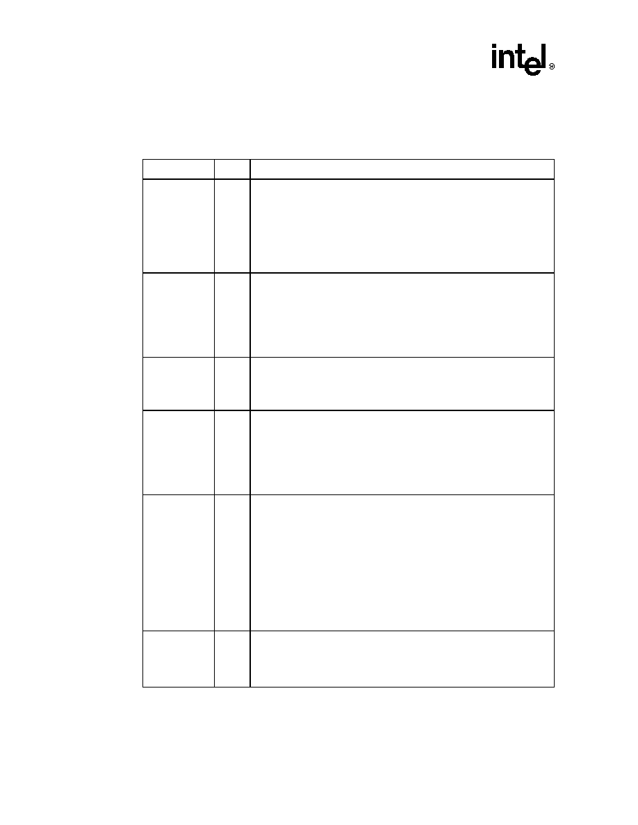
Table 25. Signal Description (Page 1 of 8)
Name
Type
Description
A[35:3]#
Input/
Output
A[35:3]# (Address) define a 236-byte physical memory address space. In
subphase 1 of the address phase, these pins transmit the address of a
transaction. In subphase 2, these pins transmit transaction type information.
These signals must connect the appropriate pins of all agents on the processor
FSB. A[35:3]# are protected by parity signals AP[1:0]#. A[35:3]# are source
synchronous signals and are latched into the receiving buffers by ADSTB[1:0]#.
On the active-to-inactive transition of RESET#, the processor samples a subset
of the A[35:3]# pins to determine power-on configuration. See Section 6.1 for
more details.
A20M#
Input
If A20M# (Address-20 Mask) is asserted, the processor masks physical address
bit 20 (A20#) before looking up a line in any internal cache and before driving a
read/write transaction on the bus. Asserting A20M# emulates the 8086
processor's address wrap-around at the 1-MB boundary. Assertion of A20M# is
only supported in real mode.
A20M# is an asynchronous signal. However, to ensure recognition of this signal
following an input/output write instruction, it must be valid along with the TRDY#
assertion of the corresponding input/output write bus transaction.
ADS#
Input/
Output
ADS# (Address Strobe) is asserted to indicate the validity of the transaction
address on the A[35:3]# and REQ[4:0]# pins. All bus agents observe the ADS#
activation to begin parity checking, protocol checking, address decode, internal
snoop, or deferred reply ID match operations associated with the new
transaction.
ADSTB[1:0]#
Input/
Output
Address strobes are used to latch A[35:3]# and REQ[4:0]# on their rising and
falling edges. Strobes are associated with signals as shown below.
AP[1:0]#
Input/
Output
AP[1:0]# (Address Parity) are driven by the request initiator along with ADS#,
A[35:3]#, and the transaction type on the REQ[4:0]#. A correct parity signal is
high if an even number of covered signals are low and low if an odd number of
covered signals are low. This allows parity to be high when all the covered
signals are high. AP[1:0]# should connect the appropriate pins of all processor
FSB agents. The following table defines the coverage model of these signals.
BCLK[1:0]
Input
The differential pair BCLK (Bus Clock) determines the FSB frequency. All
processor FSB agents must receive these signals to drive their outputs and latch
their inputs.
All external timing parameters are specified with respect to the rising edge of
BCLK0 crossing VCROSS.
Signals
Associated Strobe
REQ[4:0]#, A[16:3]#
ADSTB0#
A[35:17]#
ADSTB1#
Request Signals
Subphase 1
Subphase 2
A[35:24]#
AP0#
AP1#
A[23:3]#
AP1#
AP0#
REQ[4:0]#
AP1#
AP0#
相关PDF资料 |
PDF描述 |
|---|---|
| RK80532RC049128 | 32-BIT, 2100 MHz, MICROPROCESSOR, CPGA478 |
| RK80532RC056128 | 2400 MHz, MICROPROCESSOR, CPGA478 |
| RK80546KG0882MM | 64-BIT, 3200 MHz, MICROPROCESSOR, CPGA604 |
| RK80546KG1042MM | 64-BIT, 3600 MHz, MICROPROCESSOR, CPGA604 |
| RK80546KG0802MM | 64-BIT, 3000 MHz, MICROPROCESSOR, CPGA604 |
相关代理商/技术参数 |
参数描述 |
|---|---|
| RK80532PG072512S L6WJ | 制造商:Intel 功能描述:MPU Pentium 制造商:Intel 功能描述:MPU Pentium? 4 Processor 64-Bit 0.13um 2.8GHz 478-Pin FCPGA2 |
| RK80532PG080512 | 制造商:Intel 功能描述:P4 3.0GHZ 800MHZ FSB - Trays |
| RK80532PG080512SL6WK | 制造商:Intel 功能描述:MPU Pentium? 4 Processor NetBurst 64-Bit 0.13um 3GHz 478-Pin FCPGA2 |
| RK80532PG0882M | 制造商:Intel 功能描述:MPU PENTIUM 4 PROCESSOR NETBURST 64-BIT 0.13UM 3.2GHZ 478-P - Trays |
| RK80532PG096512 | 制造商:Intel 功能描述:MPU PENTIUM 4 PROCESSOR NETBURST 64-BIT 0.13UM 3.4GHZ - Trays |
发布紧急采购,3分钟左右您将得到回复。