- 您现在的位置:买卖IC网 > PDF目录98069 > S1D13806F00A CRT OR FLAT PNL GRPH DSPL CTLR, PQFP144 PDF资料下载
参数资料
| 型号: | S1D13806F00A |
| 元件分类: | 显示控制器 |
| 英文描述: | CRT OR FLAT PNL GRPH DSPL CTLR, PQFP144 |
| 封装: | QFP-144 |
| 文件页数: | 146/352页 |
| 文件大小: | 3748K |
| 代理商: | S1D13806F00A |
第1页第2页第3页第4页第5页第6页第7页第8页第9页第10页第11页第12页第13页第14页第15页第16页第17页第18页第19页第20页第21页第22页第23页第24页第25页第26页第27页第28页第29页第30页第31页第32页第33页第34页第35页第36页第37页第38页第39页第40页第41页第42页第43页第44页第45页第46页第47页第48页第49页第50页第51页第52页第53页第54页第55页第56页第57页第58页第59页第60页第61页第62页第63页第64页第65页第66页第67页第68页第69页第70页第71页第72页第73页第74页第75页第76页第77页第78页第79页第80页第81页第82页第83页第84页第85页第86页第87页第88页第89页第90页第91页第92页第93页第94页第95页第96页第97页第98页第99页第100页第101页第102页第103页第104页第105页第106页第107页第108页第109页第110页第111页第112页第113页第114页第115页第116页第117页第118页第119页第120页第121页第122页第123页第124页第125页第126页第127页第128页第129页第130页第131页第132页第133页第134页第135页第136页第137页第138页第139页第140页第141页第142页第143页第144页第145页当前第146页第147页第148页第149页第150页第151页第152页第153页第154页第155页第156页第157页第158页第159页第160页第161页第162页第163页第164页第165页第166页第167页第168页第169页第170页第171页第172页第173页第174页第175页第176页第177页第178页第179页第180页第181页第182页第183页第184页第185页第186页第187页第188页第189页第190页第191页第192页第193页第194页第195页第196页第197页第198页第199页第200页第201页第202页第203页第204页第205页第206页第207页第208页第209页第210页第211页第212页第213页第214页第215页第216页第217页第218页第219页第220页第221页第222页第223页第224页第225页第226页第227页第228页第229页第230页第231页第232页第233页第234页第235页第236页第237页第238页第239页第240页第241页第242页第243页第244页第245页第246页第247页第248页第249页第250页第251页第252页第253页第254页第255页第256页第257页第258页第259页第260页第261页第262页第263页第264页第265页第266页第267页第268页第269页第270页第271页第272页第273页第274页第275页第276页第277页第278页第279页第280页第281页第282页第283页第284页第285页第286页第287页第288页第289页第290页第291页第292页第293页第294页第295页第296页第297页第298页第299页第300页第301页第302页第303页第304页第305页第306页第307页第308页第309页第310页第311页第312页第313页第314页第315页第316页第317页第318页第319页第320页第321页第322页第323页第324页第325页第326页第327页第328页第329页第330页第331页第332页第333页第334页第335页第336页第337页第338页第339页第340页第341页第342页第343页第344页第345页第346页第347页第348页第349页第350页第351页第352页
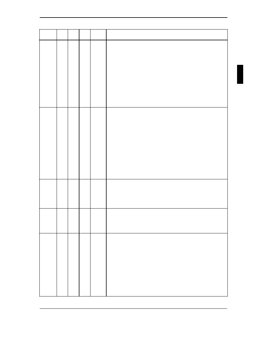
4: PINS
S1D13806 SERIES HARDWARE FUNCTIONAL
EPSON
1-11
SPECIFICATION (X28B-A-001-03)
DB[15:0]
IO
40-55 C/TS2
Hi-Z
These pins are the system data bus.
For SH-3/SH-4 Bus, these pins are connected to D[15:0].
For MC68K Bus 1, these pins are connected to D[15:0].
For MC68K Bus 2, these pins are connected to D[31:16] for 32-bit devices
(e.g. MC68030) or D[15:0] for 16-bit devices (e.g. MC68340).
For Generic Bus, these pins are connected to D[15:0].
For MIPS/ISA Bus, these pins are connected to SD[15:0].
For Philips PR31500/31700 Bus, pins DB[15:8] are connected to D[23:16] and
pins DB[7:0] are connected to D[31:24].
For Toshiba TX39xx Bus, pins DB[15:8] are connected to D[23:16] and pins
DB[7:0] are connected to D[31:24].
For PowerPC Bus, these pins are connected to D[0:15].
For PC Card (PCMCIA) Bus, these pins are connected to D[15:0].
See Table 4-9, “CPU Interface Pin Mapping,” on page 18 for summary.
See the respective AC Timing diagram for detailed functionality.
WE1#
IO
33
CS/
TS2
Hi-Z
This is a multi-purpose pin:
For SH-3/SH-4 Bus, this pin inputs the write enable signal for the upper data byte
(WE1#).
For MC68K Bus 1, this pin inputs the upper data strobe (UDS#).
For MC68K Bus 2, this pin inputs the data strobe (DS#).
For Generic Bus, this pin inputs the write enable signal for the upper data byte
(WE1#).
For MIPS/ISA Bus, this pin inputs the system byte high enable signal (SBHE#).
For Philips PR31500/31700 Bus, this pin inputs the odd byte access enable signal
(/CARDxCSH).
For Toshiba TX39xx Bus, this pin inputs the odd byte access enable signal
(CARDxCSH*).
For PowerPC Bus, this pin outputs the burst inhibit signal (BI#).
For PC Card (PCMCIA) Bus, this pin inputs the card enable 2 signal (-CE2).
See Table 4-9, “CPU Interface Pin Mapping,” on page 18 for summary.
See the respective AC Timing diagram for detailed functionality.
M/R#
I
29
C
Hi-Z
For Philips PR31500/31700 Bus, this pin is connected to VDD.
For Toshiba TX39xx Bus, this pin is connected to VDD.
For all other busses, this input pin is used to select between the display buffer and
register address spaces of the S1D13806. M/R# is set high to access the display
buffer and low to access the registers. See Register Mapping.
CS#
I
28
C
Hi-Z
For Philips PR31500/31700 Bus, this pin is connected to VDD.
For Toshiba TX39xx Bus, this pin is connected to VDD.
For all other busses, this is the Chip Select input.
See the respective AC Timing diagram for detailed functionality.
BUSCLK
I
60
C
Hi-Z
This pin inputs the system bus clock. It is possible to apply a 2x clock and divide it
by 2 internally - see CONF5 in Summary of Configuration Options.
For SH-3/SH-4 Bus, this pin is connected to CKIO.
For MC68K Bus 1, this pin is connected to CLK.
For MC68K Bus 2, this pin is connected to CLK.
For Generic Bus, this pin is connected to BCLK.
For MIPS/ISA Bus, this pin is connected to CLK.
For Philips PR31500/31700 Bus, this pin is connected to DCLKOUT.
For Toshiba TX39xx Bus, this pin is connected to DCLKOUT.
For PowerPC Bus, this pin is connected to CLKOUT.
For PC Card (PCMCIA) Bus, this pin is connected to the input clock
(CLKI, pin 69).
See Table 4-9, “CPU Interface Pin Mapping,” on page 18 for summary.
See the respective AC Timing diagram for detailed functionality.
Table 4-1 Host Interface Pin Descriptions (Continued)
Pin Name Type
Pin #
Cell
RESET#
State
Description
相关PDF资料 |
PDF描述 |
|---|---|
| S1D13A05B00B | 320 X 320 PIXELS CRT OR FLAT PNL GRPH DSPL CTLR, PBGA121 |
| S1D13A05F00A100 | 320 X 320 PIXELS CRT OR FLAT PNL GRPH DSPL CTLR, PBGA121 |
| S1R72005F00A300 | UNIVERSAL SERIAL BUS CONTROLLER, PQFP64 |
| S1R72105F00A000 | SCSI BUS CONTROLLER, PQFP100 |
| S1R72803F00A100 | 1 CHANNEL(S), 400M bps, SERIAL COMM CONTROLLER, PQFP100 |
相关代理商/技术参数 |
参数描述 |
|---|---|
| S1D13806F00A100 | 制造商:Epson Electronics America Inc 功能描述: |
| S1D13A03B00B | 制造商:EPSON 制造商全称:EPSON 功能描述:LCD Controller ICs |
| S1D13A03B00B200 | 功能描述:IC LCD COMPANION 112K 121-PFBGA RoHS:否 类别:集成电路 (IC) >> PMIC - 显示器驱动器 系列:- 产品培训模块:Lead (SnPb) Finish for COTS Obsolescence Mitigation Program 标准包装:2,500 系列:- 显示器类型:真空荧光 (VF) 配置:5 x 7(矩阵) 接口:串行 数字或字符:- 电流 - 电源:3.5mA 电源电压:2.7 V ~ 3.6 V 工作温度:-40°C ~ 125°C 安装类型:表面贴装 封装/外壳:16-SSOP(0.154",3.90mm 宽) 供应商设备封装:16-QSOP 包装:带卷 (TR) |
| S1D13A03F00A | 制造商:EPSON 制造商全称:EPSON 功能描述:LCD Controller ICs |
| S1D13A04B00B | 制造商:EPSON 制造商全称:EPSON 功能描述:LCD Controller ICs |
发布紧急采购,3分钟左右您将得到回复。