- 您现在的位置:买卖IC网 > PDF目录270896 > S75PL127JCDBFWB0 (Spansion Inc.) Power supply woltage of 2.7 to 3.1 volt PDF资料下载
参数资料
| 型号: | S75PL127JCDBFWB0 |
| 厂商: | Spansion Inc. |
| 英文描述: | Power supply woltage of 2.7 to 3.1 volt |
| 中文描述: | 功率2月7号至三月一日伏的电源woltage |
| 文件页数: | 130/183页 |
| 文件大小: | 4247K |
| 代理商: | S75PL127JCDBFWB0 |
第1页第2页第3页第4页第5页第6页第7页第8页第9页第10页第11页第12页第13页第14页第15页第16页第17页第18页第19页第20页第21页第22页第23页第24页第25页第26页第27页第28页第29页第30页第31页第32页第33页第34页第35页第36页第37页第38页第39页第40页第41页第42页第43页第44页第45页第46页第47页第48页第49页第50页第51页第52页第53页第54页第55页第56页第57页第58页第59页第60页第61页第62页第63页第64页第65页第66页第67页第68页第69页第70页第71页第72页第73页第74页第75页第76页第77页第78页第79页第80页第81页第82页第83页第84页第85页第86页第87页第88页第89页第90页第91页第92页第93页第94页第95页第96页第97页第98页第99页第100页第101页第102页第103页第104页第105页第106页第107页第108页第109页第110页第111页第112页第113页第114页第115页第116页第117页第118页第119页第120页第121页第122页第123页第124页第125页第126页第127页第128页第129页当前第130页第131页第132页第133页第134页第135页第136页第137页第138页第139页第140页第141页第142页第143页第144页第145页第146页第147页第148页第149页第150页第151页第152页第153页第154页第155页第156页第157页第158页第159页第160页第161页第162页第163页第164页第165页第166页第167页第168页第169页第170页第171页第172页第173页第174页第175页第176页第177页第178页第179页第180页第181页第182页第183页
August 12, 2004 S29PL127J_064J_032J_MCP_00_A3
S29PL127J/S29PL064J/S29PL032J for MCP
51
Prel imin ary
CFI Query (Note 13)
1
55
98
Accelerated Program (Note 15)
2
XX
A0
PA
PD
Unlock Bypass Entry (Note 15)
3
555
AA
2AA
55
555
20
Unlock Bypass Program (Note 15)
2
XX
A0
PA
PD
Unlock Bypass Erase (Note 15)
2
XX
80
XX
10
Unlock Bypass CFI (Notes 13, 15)
1
XX
98
Unlock Bypass Reset (Note 15)
2
XXX
90
XXX
00
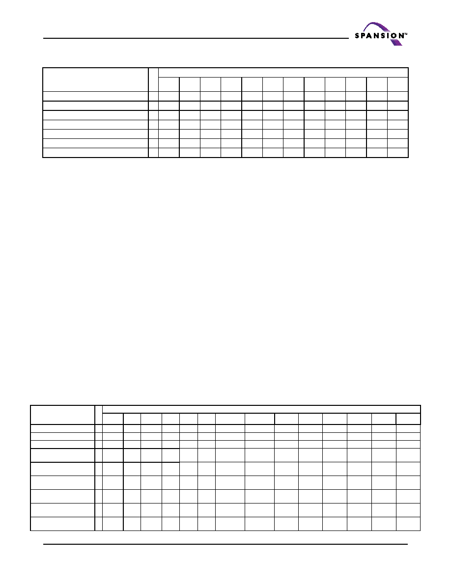
Table 14. Sector Protection Command Definitions
Command (Notes)
Cyc
les
Bus Cycles (Notes 1-4)
Addr Data Addr Data Addr Data
Addr
Data
Addr
Data
Addr
Data
Addr
Data
Reset
1
XXX
F0
SecSi Sector Entry
3
555
AA
2AA
55
555
88
SecSi Sector Exit
4
555
AA
2AA
55
555
90
XX
00
SecSi Protection Bit
6
555
AA
2AA
55
555
60
OW
68
OW
48
OW
RD(0)
SecSi Protection Bit
Status
5
555
AA
2AA
55
555
60
OW
48
OW
RD(0)
Password Program
(Notes 5, 7, 8)
4
555
AA
2AA
55
555
38
XX[0-3]
PD[0-3]
Password Verify (Notes
4
555
AA
2AA
55
555
C8
PWA[0-3] PWD[0-3]
Password Unlock (Notes
7
555
AA
2AA
55
555
28
PWA[0]
PWD[0]
PWA[1] PWD[1] PWA[2] PWD[2] PWA[3] PWD[3]
PPB Program (Notes 5,
6
555
AA
2AA
55
555
60
(SA)WP
68
(SA)WP
48
(SA)WP
RD(0)
Table 13. Memory Array Command Definitions
Command (Notes)
Cy
cl
e
s
Bus Cycles (Notes 1–4)
Addr
Data
Addr
Data
Addr
Data
Addr
Data
Addr
Data
Addr
Data
Legend:
BA = Address of bank switching to autoselect mode, bypass
mode, or erase operation. Determined by PL127J: Amax:A20,
PL064J: Amax:A19, PL032J: Amax:A18.
PA = Program Address (Amax:A0). Addresses latch on falling
edge of WE# or CE# pulse, whichever happens later.
PD = Program Data (DQ15:DQ0) written to location PA. Data
latches on rising edge of WE# or CE# pulse, whichever happens
first.
RA = Read Address (Amax:A0).
RD = Read Data (DQ15:DQ0) from location RA.
SA = Sector Address (Amax:A12) for verifying (in autoselect
mode) or erasing.
WD = Write Data. See “Configuration Register” definition for
specific write data. Data latched on rising edge of WE#.
X = Don’t care
Notes:
1. See Table 1 for description of bus operations.
2. All values are in hexadecimal.
3. Shaded cells in table denote read cycles. All other cycles are
write operations.
4. During unlock and command cycles, when lower address bits
are 555 or 2AAh as shown in table, address bits higher than
A11 (except where BA is required) and data bits higher than
DQ7 are don’t cares.
5. No unlock or command cycles required when bank is reading
array data.
6. The Reset command is required to return to reading array
(or to erase-suspend-read mode if previously in Erase
Suspend) when bank is in autoselect mode, or if DQ5 goes
high (while bank is providing status information).
7. Fourth cycle of autoselect command sequence is a read
cycle. System must provide bank address to obtain
manufacturer ID or device ID information. See Autoselect
Command Sequence section for more information.
8. The data is C4h for factory and customer locked, 84h for
factory locked and 04h for not locked.
9. The data is 00h for an unprotected sector group and 01h for
a protected sector group.
10. Device ID must be read across cycles 4, 5, and 6. PL127J
(X0Eh = 2220h, X0Fh = 2200h),PL064J (X0Eh = 2202h,
X0Fh = 2201h), PL032J (X0Eh = 220Ah, X0Fh = 2201h).
11. System may read and program in non-erasing sectors, or
enter autoselect mode, when in Program/Erase Suspend
mode. Program/Erase Suspend command is valid only
during a sector erase operation, and requires bank address.
12. Program/Erase Resume command is valid only during Erase
Suspend mode, and requires bank address.
13. Command is valid when device is ready to read array data or
when device is in autoselect mode.
14. WP#/ACC must be at VID during the entire operation of
command.
15. Unlock Bypass Entry command is required prior to any
Unlock Bypass operation. Unlock Bypass Reset command is
required to return to the reading array.
相关PDF资料 |
PDF描述 |
|---|---|
| S75PL127JCDBFWB2 | Power supply woltage of 2.7 to 3.1 volt |
| S75PL127JCEBFWB2 | Power supply woltage of 2.7 to 3.1 volt |
| S75PL127JCDBFWB3 | Power supply woltage of 2.7 to 3.1 volt |
| S75PL127JCEBFWB3 | Power supply woltage of 2.7 to 3.1 volt |
| S29CD016G0PFAN010 | 16 Megabit (512 K x 32-Bit) CMOS 2.5 Volt-only Burst Mode, Dual Boot, Simultaneous Read/Write Flash Memory |
相关代理商/技术参数 |
参数描述 |
|---|---|
| S75PL127JCDBFWB2 | 制造商:SPANSION 制造商全称:SPANSION 功能描述:Power supply woltage of 2.7 to 3.1 volt |
| S75PL127JCDBFWB3 | 制造商:SPANSION 制造商全称:SPANSION 功能描述:Power supply woltage of 2.7 to 3.1 volt |
| S75PL127JCDBFWU0 | 制造商:SPANSION 制造商全称:SPANSION 功能描述:Power supply woltage of 2.7 to 3.1 volt |
| S75PL127JCDBFWU2 | 制造商:SPANSION 制造商全称:SPANSION 功能描述:Power supply woltage of 2.7 to 3.1 volt |
| S75PL127JCDBFWU3 | 制造商:SPANSION 制造商全称:SPANSION 功能描述:Power supply woltage of 2.7 to 3.1 volt |
发布紧急采购,3分钟左右您将得到回复。