- 您现在的位置:买卖IC网 > PDF目录270896 > S75PL127JCDBFWB0 (Spansion Inc.) Power supply woltage of 2.7 to 3.1 volt PDF资料下载
参数资料
| 型号: | S75PL127JCDBFWB0 |
| 厂商: | Spansion Inc. |
| 英文描述: | Power supply woltage of 2.7 to 3.1 volt |
| 中文描述: | 功率2月7号至三月一日伏的电源woltage |
| 文件页数: | 71/183页 |
| 文件大小: | 4247K |
| 代理商: | S75PL127JCDBFWB0 |
第1页第2页第3页第4页第5页第6页第7页第8页第9页第10页第11页第12页第13页第14页第15页第16页第17页第18页第19页第20页第21页第22页第23页第24页第25页第26页第27页第28页第29页第30页第31页第32页第33页第34页第35页第36页第37页第38页第39页第40页第41页第42页第43页第44页第45页第46页第47页第48页第49页第50页第51页第52页第53页第54页第55页第56页第57页第58页第59页第60页第61页第62页第63页第64页第65页第66页第67页第68页第69页第70页当前第71页第72页第73页第74页第75页第76页第77页第78页第79页第80页第81页第82页第83页第84页第85页第86页第87页第88页第89页第90页第91页第92页第93页第94页第95页第96页第97页第98页第99页第100页第101页第102页第103页第104页第105页第106页第107页第108页第109页第110页第111页第112页第113页第114页第115页第116页第117页第118页第119页第120页第121页第122页第123页第124页第125页第126页第127页第128页第129页第130页第131页第132页第133页第134页第135页第136页第137页第138页第139页第140页第141页第142页第143页第144页第145页第146页第147页第148页第149页第150页第151页第152页第153页第154页第155页第156页第157页第158页第159页第160页第161页第162页第163页第164页第165页第166页第167页第168页第169页第170页第171页第172页第173页第174页第175页第176页第177页第178页第179页第180页第181页第182页第183页
December 15, 2004 S29GLxxxN_MCP_A1
S29GLxxxN MirrorBitTM Flash Family
163
Advance
Informatio n
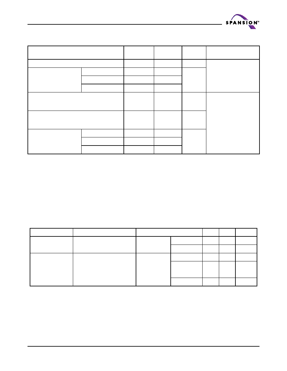
Erase And Programming Performance
Notes:
1. Typical program and erase times assume the following conditions: 25°C, 3.0 V VCC, 10,000 cycles, checkerboard
pattern.
2. Under worst case conditions of 90°C, VCC = 3.0 V, 100,000 cycles.
3. Effective write buffer specification is based upon a 16-word write buffer operation.
4. The typical chip programming time is considerably less than the maximum chip programming time listed, since most
words program faster than the maximum program times listed.
5. In the pre-programming step of the Embedded Erase algorithm, all bits are programmed to 00h before erasure.
6. System-level overhead is the time required to execute the two- or four-bus-cycle sequence for the program
command. See Table 12 for further information on command definitions.
TSOP Pin and BGA Package Capacitance
Notes:
1. Sampled, not 100% tested.
2. Test conditions TA = 25°C, f = 1.0 MHz.
Parameter
Typ
(Note 1)
Max
(Note 2)
Unit
Comments
Sector Erase Time
0.5
3.5
sec
Excludes 00h
programming prior to
erasure (Note 5)
Chip Erase Time
S29GL128N
64
256
sec
S29GL256N
128
512
S29GL512N
256
1024
Total Write Buffer
Programming Time
(Note 3)
240
s
Excludes system level
overhead (Note 6)
Total Accelerated Effective
Write Buffer Programming
Time (Note 3)
200
s
Chip Program Time
S29GL128N
123
sec
S29GL256N
246
S29GL512N
492
Parameter Symbol
Parameter Description
Test Setup
Typ
Max
Unit
CIN
Input Capacitance
VIN = 0
TSOP
6
7.5
pF
BGA
4.2
5.0
pF
COUT
Output Capacitance
VOUT = 0
TSOP
8.5
12
pF
BGA
5.4
6.5
pF
CIN2
Control Pin Capacitance
VIN = 0
TSOP
7.5
9
pF
BGA
3.9
4.7
pF
相关PDF资料 |
PDF描述 |
|---|---|
| S75PL127JCDBFWB2 | Power supply woltage of 2.7 to 3.1 volt |
| S75PL127JCEBFWB2 | Power supply woltage of 2.7 to 3.1 volt |
| S75PL127JCDBFWB3 | Power supply woltage of 2.7 to 3.1 volt |
| S75PL127JCEBFWB3 | Power supply woltage of 2.7 to 3.1 volt |
| S29CD016G0PFAN010 | 16 Megabit (512 K x 32-Bit) CMOS 2.5 Volt-only Burst Mode, Dual Boot, Simultaneous Read/Write Flash Memory |
相关代理商/技术参数 |
参数描述 |
|---|---|
| S75PL127JCDBFWB2 | 制造商:SPANSION 制造商全称:SPANSION 功能描述:Power supply woltage of 2.7 to 3.1 volt |
| S75PL127JCDBFWB3 | 制造商:SPANSION 制造商全称:SPANSION 功能描述:Power supply woltage of 2.7 to 3.1 volt |
| S75PL127JCDBFWU0 | 制造商:SPANSION 制造商全称:SPANSION 功能描述:Power supply woltage of 2.7 to 3.1 volt |
| S75PL127JCDBFWU2 | 制造商:SPANSION 制造商全称:SPANSION 功能描述:Power supply woltage of 2.7 to 3.1 volt |
| S75PL127JCDBFWU3 | 制造商:SPANSION 制造商全称:SPANSION 功能描述:Power supply woltage of 2.7 to 3.1 volt |
发布紧急采购,3分钟左右您将得到回复。