- 您现在的位置:买卖IC网 > PDF目录270896 > S75PL127JCDBFWB0 (Spansion Inc.) Power supply woltage of 2.7 to 3.1 volt PDF资料下载
参数资料
| 型号: | S75PL127JCDBFWB0 |
| 厂商: | Spansion Inc. |
| 英文描述: | Power supply woltage of 2.7 to 3.1 volt |
| 中文描述: | 功率2月7号至三月一日伏的电源woltage |
| 文件页数: | 131/183页 |
| 文件大小: | 4247K |
| 代理商: | S75PL127JCDBFWB0 |
第1页第2页第3页第4页第5页第6页第7页第8页第9页第10页第11页第12页第13页第14页第15页第16页第17页第18页第19页第20页第21页第22页第23页第24页第25页第26页第27页第28页第29页第30页第31页第32页第33页第34页第35页第36页第37页第38页第39页第40页第41页第42页第43页第44页第45页第46页第47页第48页第49页第50页第51页第52页第53页第54页第55页第56页第57页第58页第59页第60页第61页第62页第63页第64页第65页第66页第67页第68页第69页第70页第71页第72页第73页第74页第75页第76页第77页第78页第79页第80页第81页第82页第83页第84页第85页第86页第87页第88页第89页第90页第91页第92页第93页第94页第95页第96页第97页第98页第99页第100页第101页第102页第103页第104页第105页第106页第107页第108页第109页第110页第111页第112页第113页第114页第115页第116页第117页第118页第119页第120页第121页第122页第123页第124页第125页第126页第127页第128页第129页第130页当前第131页第132页第133页第134页第135页第136页第137页第138页第139页第140页第141页第142页第143页第144页第145页第146页第147页第148页第149页第150页第151页第152页第153页第154页第155页第156页第157页第158页第159页第160页第161页第162页第163页第164页第165页第166页第167页第168页第169页第170页第171页第172页第173页第174页第175页第176页第177页第178页第179页第180页第181页第182页第183页
52
S29PL127J/S29PL064J/S29PL032J for MCP
S29PL127J_064J_032J_MCP_00_A3 August 12, 2004
Preli m inary
Write Operation Status
The device provides several bits to determine the status of a program or erase opera-
tion: DQ2, DQ3, DQ5, DQ6, and DQ7. Table 15 and the following subsections describe
the function of these bits. DQ7 and DQ6 each offer a method for determining whether
a program or erase operation is complete or in progress. The device also provides a
hardware-based output signal, RY/BY#, to determine whether an Embedded Program
or Erase operation is in progress or has been completed.
DQ7: Data# Polling
The Data# Polling bit, DQ7, indicates to the host system whether an Embedded Pro-
gram or Erase algorithm is in progress or completed, or whether a bank is in Erase
Suspend. Data# Polling is valid after the rising edge of the final WE# pulse in the com-
mand sequence.
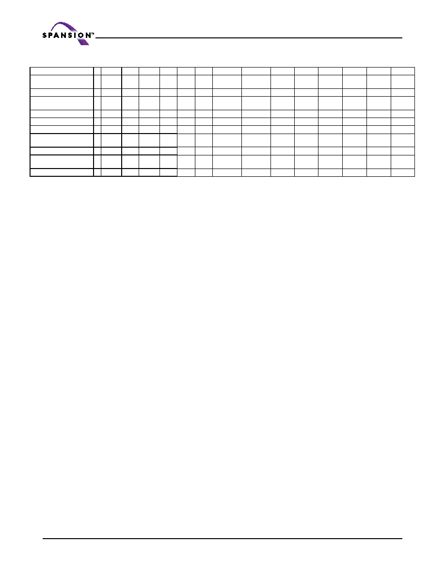
PPB Status
4
555
AA
2AA
55
555
90
(SA)WP
RD(0)
All PPB Erase (Notes 5,
6
555
AA
2AA
55
555
60
WP
60
(SA)
40
(SA)WP
RD(0)
PPB Lock Bit Set
3
555
AA
2AA
55
555
78
PPB Lock Bit Status
4
555
AA
2AA
55
555
58
SA
RD(1)
DYB Write (Note 7)
4
555
AA
2AA
55
555
48
SA
X1
DYB Erase (Note 7)
4
555
AA
2AA
55
555
48
SA
X0
DYB Status (Note 6)
4
555
AA
2AA
55
555
58
SA
RD(0)
PPMLB Program (Notes
6
555
AA
2AA
55
555
60
PL
68
PL
48
PL
RD(0)
PPMLB Status (Note 5)
5
555
AA
2AA
55
555
60
PL
48
PL
RD(0)
SPMLB Program (Notes
6
555
AA
2AA
55
555
60
SL
68
SL
48
SL
RD(0)
SPMLB Status (Note 5)
5
555
AA
2AA
55
555
60
SL
48
SL
RD(0)
Table 14. Sector Protection Command Definitions
Legend:
DYB = Dynamic Protection Bit
OW = Address (A7:A0) is (00011010)
PD[3:0] = Password Data (1 of 4 portions)
PPB = Persistent Protection Bit
PWA = Password Address. A1:A0 selects portion of password.
PWD = Password Data being verified.
PL = Password Protection Mode Lock Address (A7:A0) is
(00001010)
RD(0) = Read Data DQ0 for protection indicator bit.
RD(1) = Read Data DQ1 for PPB Lock status.
SA = Sector Address where security command applies. Address
bits Amax:A12 uniquely select any sector.
SL = Persistent Protection Mode Lock Address (A7:A0) is
(00010010)
WP = PPB Address (A7:A0) is (00000010)
X = Don’t care
PPMLB = Password Protection Mode Locking Bit
SPMLB = Persistent Protection Mode Locking Bit
Notes:
1. See Table 1 for description of bus operations.
2. All values are in hexadecimal.
3. Shaded cells in table denote read cycles. All other cycles are
write operations.
4. During unlock and command cycles, when lower address bits
are 555 or 2AAh as shown in table, address bits higher than
A11 (except where BA is required) and data bits higher than
DQ7 are don’t cares.
5. The reset command returns device to reading array.
6. Cycle 4 programs the addressed locking bit. Cycles 5 and 6
validate bit has been fully programmed when DQ0 = 1. If
DQ0 = 0 in cycle 6, program command must be issued and
verified again.
7. Data is latched on the rising edge of WE#.
8. Entire command sequence must be entered for each portion
of password.
9. Command sequence returns FFh if PPMLB is set.
10. The password is written over four consecutive cycles, at
addresses 0-3.
11. A 2 s timeout is required between any two portions of
password.
12. A 100 s timeout is required between cycles 4 and 5.
13. A 1.2 ms timeout is required between cycles 4 and 5.
14. Cycle 4 erases all PPBs. Cycles 5 and 6 validate bits have
been fully erased when DQ0 = 0. If DQ0 = 1 in cycle 6,
erase command must be issued and verified again. Before
issuing erase command, all PPBs should be programmed to
prevent PPB overerasure.
15. DQ1 = 1 if PPB locked, 0 if unlocked.
相关PDF资料 |
PDF描述 |
|---|---|
| S75PL127JCDBFWB2 | Power supply woltage of 2.7 to 3.1 volt |
| S75PL127JCEBFWB2 | Power supply woltage of 2.7 to 3.1 volt |
| S75PL127JCDBFWB3 | Power supply woltage of 2.7 to 3.1 volt |
| S75PL127JCEBFWB3 | Power supply woltage of 2.7 to 3.1 volt |
| S29CD016G0PFAN010 | 16 Megabit (512 K x 32-Bit) CMOS 2.5 Volt-only Burst Mode, Dual Boot, Simultaneous Read/Write Flash Memory |
相关代理商/技术参数 |
参数描述 |
|---|---|
| S75PL127JCDBFWB2 | 制造商:SPANSION 制造商全称:SPANSION 功能描述:Power supply woltage of 2.7 to 3.1 volt |
| S75PL127JCDBFWB3 | 制造商:SPANSION 制造商全称:SPANSION 功能描述:Power supply woltage of 2.7 to 3.1 volt |
| S75PL127JCDBFWU0 | 制造商:SPANSION 制造商全称:SPANSION 功能描述:Power supply woltage of 2.7 to 3.1 volt |
| S75PL127JCDBFWU2 | 制造商:SPANSION 制造商全称:SPANSION 功能描述:Power supply woltage of 2.7 to 3.1 volt |
| S75PL127JCDBFWU3 | 制造商:SPANSION 制造商全称:SPANSION 功能描述:Power supply woltage of 2.7 to 3.1 volt |
发布紧急采购,3分钟左右您将得到回复。