- 您现在的位置:买卖IC网 > PDF目录270896 > S75PL127JCDBFWB0 (Spansion Inc.) Power supply woltage of 2.7 to 3.1 volt PDF资料下载
参数资料
| 型号: | S75PL127JCDBFWB0 |
| 厂商: | Spansion Inc. |
| 英文描述: | Power supply woltage of 2.7 to 3.1 volt |
| 中文描述: | 功率2月7号至三月一日伏的电源woltage |
| 文件页数: | 51/183页 |
| 文件大小: | 4247K |
| 代理商: | S75PL127JCDBFWB0 |
第1页第2页第3页第4页第5页第6页第7页第8页第9页第10页第11页第12页第13页第14页第15页第16页第17页第18页第19页第20页第21页第22页第23页第24页第25页第26页第27页第28页第29页第30页第31页第32页第33页第34页第35页第36页第37页第38页第39页第40页第41页第42页第43页第44页第45页第46页第47页第48页第49页第50页当前第51页第52页第53页第54页第55页第56页第57页第58页第59页第60页第61页第62页第63页第64页第65页第66页第67页第68页第69页第70页第71页第72页第73页第74页第75页第76页第77页第78页第79页第80页第81页第82页第83页第84页第85页第86页第87页第88页第89页第90页第91页第92页第93页第94页第95页第96页第97页第98页第99页第100页第101页第102页第103页第104页第105页第106页第107页第108页第109页第110页第111页第112页第113页第114页第115页第116页第117页第118页第119页第120页第121页第122页第123页第124页第125页第126页第127页第128页第129页第130页第131页第132页第133页第134页第135页第136页第137页第138页第139页第140页第141页第142页第143页第144页第145页第146页第147页第148页第149页第150页第151页第152页第153页第154页第155页第156页第157页第158页第159页第160页第161页第162页第163页第164页第165页第166页第167页第168页第169页第170页第171页第172页第173页第174页第175页第176页第177页第178页第179页第180页第181页第182页第183页
December 15, 2004 S29GLxxxN_MCP_A1
S29GLxxxN MirrorBitTM Flash Family
145
Advance
Informatio n
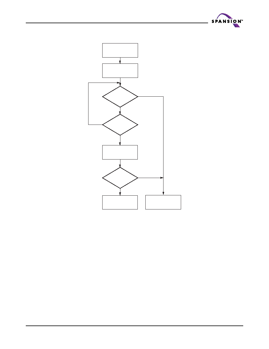
Figure 5. Data# Polling Algorithm
RY/BY#: Ready/Busy#
The RY/BY# is a dedicated, open-drain output pin which indicates whether an
Embedded Algorithm is in progress or complete. The RY/BY# status is valid after
the rising edge of the final WE# pulse in the command sequence. Since RY/BY#
is an open-drain output, several RY/BY# pins can be tied together in parallel with
a pull-up resistor to VCC.
If the output is low (Busy), the device is actively erasing or programming. (This
includes programming in the Erase Suspend mode.) If the output is high (Ready),
the device is in the read mode, the standby mode, or in the erase-suspend-read
mode. Table 13 shows the outputs for RY/BY#.
DQ7 = Data?
Yes
No
DQ5 = 1
No
Yes
FAIL
PASS
Read DQ15–DQ0
Addr = VA
Read DQ15–DQ0
Addr = VA
DQ7 = Data?
START
Notes:
1. VA = Valid address for programming. During a sector
erase operation, a valid address is any sector address
within the sector being erased. During chip erase, a
valid address is any non-protected sector address.
2. DQ7 should be rechecked even if DQ5 = “1” because
DQ7 may change simultaneously with DQ5.
相关PDF资料 |
PDF描述 |
|---|---|
| S75PL127JCDBFWB2 | Power supply woltage of 2.7 to 3.1 volt |
| S75PL127JCEBFWB2 | Power supply woltage of 2.7 to 3.1 volt |
| S75PL127JCDBFWB3 | Power supply woltage of 2.7 to 3.1 volt |
| S75PL127JCEBFWB3 | Power supply woltage of 2.7 to 3.1 volt |
| S29CD016G0PFAN010 | 16 Megabit (512 K x 32-Bit) CMOS 2.5 Volt-only Burst Mode, Dual Boot, Simultaneous Read/Write Flash Memory |
相关代理商/技术参数 |
参数描述 |
|---|---|
| S75PL127JCDBFWB2 | 制造商:SPANSION 制造商全称:SPANSION 功能描述:Power supply woltage of 2.7 to 3.1 volt |
| S75PL127JCDBFWB3 | 制造商:SPANSION 制造商全称:SPANSION 功能描述:Power supply woltage of 2.7 to 3.1 volt |
| S75PL127JCDBFWU0 | 制造商:SPANSION 制造商全称:SPANSION 功能描述:Power supply woltage of 2.7 to 3.1 volt |
| S75PL127JCDBFWU2 | 制造商:SPANSION 制造商全称:SPANSION 功能描述:Power supply woltage of 2.7 to 3.1 volt |
| S75PL127JCDBFWU3 | 制造商:SPANSION 制造商全称:SPANSION 功能描述:Power supply woltage of 2.7 to 3.1 volt |
发布紧急采购,3分钟左右您将得到回复。