- 您现在的位置:买卖IC网 > PDF目录11815 > SC28C94A1N,112 (NXP Semiconductors)IC UART QUAD W/FIFO 48-DIP PDF资料下载
参数资料
| 型号: | SC28C94A1N,112 |
| 厂商: | NXP Semiconductors |
| 文件页数: | 35/39页 |
| 文件大小: | 0K |
| 描述: | IC UART QUAD W/FIFO 48-DIP |
| 标准包装: | 7 |
| 特点: | 故障启动位检测 |
| 通道数: | 4,QUART |
| FIFO's: | 8 字节 |
| 电源电压: | 5V |
| 带自动流量控制功能: | 是 |
| 带故障启动位检测功能: | 是 |
| 带调制解调器控制功能: | 是 |
| 带CMOS: | 是 |
| 安装类型: | 通孔 |
| 封装/外壳: | 48-DIP(0.600",15.24mm) |
| 供应商设备封装: | 48-DIP |
| 包装: | 管件 |
| 其它名称: | 568-1115-5 935262535112 SC28C94A1N |
第1页第2页第3页第4页第5页第6页第7页第8页第9页第10页第11页第12页第13页第14页第15页第16页第17页第18页第19页第20页第21页第22页第23页第24页第25页第26页第27页第28页第29页第30页第31页第32页第33页第34页当前第35页第36页第37页第38页第39页
Philips Semiconductors
Product data sheet
SC28C94
Quad universal asynchronous receiver/transmitter (QUART)
2006 Aug 09
5
PIN DESCRIPTION
MNEMONIC
TYPE
NAME AND FUNCTION
CEN
I
Chip Select: Active low input that, in conjunction with RDN or WRN, indicates that the host MPU is trying to
access a QUART register. CEN must be inactive when IACKN is asserted.
A5:0
I
Address Lines: These inputs select a 28C94 register to be read or written by the host MPU.
D7:0
I/O
8-bit Bidirectional Data Bus: Used by the host MPU to read and write 28C94 registers.
RDN
I
Read Strobe: Active low input. When this line is asserted simultaneously with CEN, the 28C94 places the
contents of the register selected by A5:0 on the D7:0 lines.
WRN
I
Write Strobe: Active low input. When this line is asserted simultaneously with CEN, the 28C94 writes the data
on D7:0 into the register selected by A5:0.
DACKN
O
Data ACKnowledge: Active low, open-drain output to the host MPU, which is asserted subsequent to a read or
write operation. For a read operation, assertion of DACKN indicates that register data is valid on D7:0. For a
write operation, it indicates that the data on D7:0 has been captured into the indicated register. This signal
corresponds to READYN on 80x86 processors and DTACKN on 680x0 processors.
IRQN
O
Interrupt Request: This active low open-drain output to the host MPU indicating that one or more of the
enabled UART interrupt sources has reached an interrupt value which exceeds that pre-programmed by host
software. The IRQN can be used directly as a 680x0 processor input; it must be inverted for use as an 80x86
interrupt input. This signal requires an external pull-up resistor.
IACKN
I
Interrupt ACKnowledge: Active low input indicates host MPU is acknowledging an interrupt requested. The
28C94 responds by placing an interrupt vector or interrupt vector modified on D7-D0 and asserting DACKN. This
signal updates the CIR register in the interrupt logic. CEN must be high during this cycle.
TDa-d
O
Transmit Data: Serial outputs from the four UARTs.
RDa-d
I
Receive Data: Serial inputs to the four UARTs/
I/O0a-d
I/O
Input/Output 0: A multi-use input or output signal for each UART. These pins can be used as general purpose
inputs, Clear to Send inputs, 1X or 16X Transmit Clock outputs or general purpose outputs. Change-of-state
detection is provided for these pins. I/O pins have approximately 1.5 Mohm pull–up device.
I/O1a-d
I/O
Input/Output 1: A multi-use input or output signal for each UART. These pins can be used as general purpose
or 1X or 16X transmit clock inputs, or general purpose 1X or 16X receive clock outputs. Change-of-state
detection is provided for these pins. In addition, I/O1a and I/O1c can be used as Counter/Timer inputs and I/O1b
and I/O1d can be used as Counter/Timer outputs. I/O pins have approximately 1.5 Mohm pull–up device.
I/O2a-d
I/O
Input/Output 2: A multi-use input or output signal for each UART. These pins can be used as general purpose
inputs, 1X or 16X receive clock inputs, general purpose outputs, RTS output or 1X or 16X receive clock outputs.
I/O pins have approximately 1.5 Mohm pull–up device.
I/O3a-d
I/O
Input/Output 3: A multi-use input or output signal for each UART. These pins can be used as general purpose
inputs, 1X or 16X transmit clock inputs, general purpose outputs, or 1X or 16X transmit clock outputs. I/O pins
have approximately 1.5 Mohm pull–up device.
RESET
I
Master Reset: Active high reset for the 28C94 logic. Must be asserted at power-up, may be asserted at other
times that the system is to be reset and restarted. OSC set to divide by 1, MR pointer set to 1, DACKN enabled,
I/O pins to input. Registers reset: MR0, OPR, CIR. IRQN, DTACKN, IVR Interrupt Vector, Power Down, Test
registers, FIFO pointers, Baud rate generator, Error Status, Watch Dog Timers, Change of State detectors,
counter/timer to timer, Transmitter and Receiver controllers and all interrupt bits. If reset pin is not used, then
first chip access should be to celar ‘power-down’ mode.
X1/CLK
I
Crystal 1 or Communication Clock: This pin is normally connected to one side of a 3.6864MHz or a
7.3728MHz crystal, or can be connected to an external clock up to 8MHz.
X2
O
Crystal 2: If a crystal is used, this pin should be connected to its other terminal. If an external clock is applied to
X1, this pin should be left unconnected.
VCC, VSS
Power and grounds: respectively.
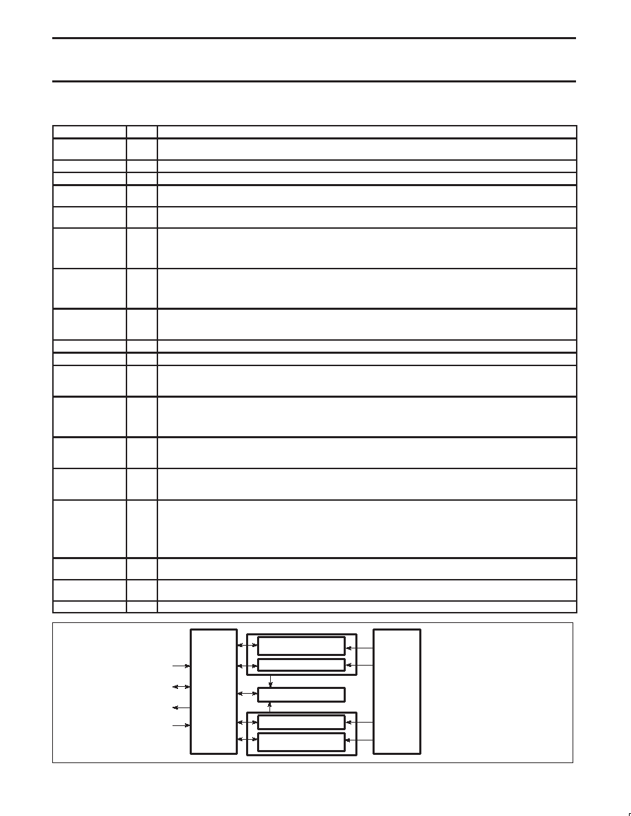
COUNTER/TIMER
I/O PORT CONTROL
UARTS A/B
INTERRUPT CONTROL
BLOCK B
UARTS C/D
I/O CONTROL
I/O PORT CONTROL
A0-A5
D (7:0)
DTACKN
IACKN
BAUD
RATE
GENERATOR
BUS
INTERFACE
BLOCK A
SD00161
Figure 3. Channel Architecture
相关PDF资料 |
PDF描述 |
|---|---|
| V24C24H150B | CONVERTER MOD DC/DC 24V 150W |
| SC16C554DIA68,512 | IC UART QUAD W/FIFO 68-PLCC |
| AT32UC3L064-D3HR | MCU AVR32 64K FLASH 48TTLGA |
| ST16C550CP40 | IC UART FIFO 16BYTE 40PDIP |
| V24B24H150BG3 | CONVERTER MOD DC/DC 24V 150W |
相关代理商/技术参数 |
参数描述 |
|---|---|
| SC28L194 | 制造商:PHILIPS 制造商全称:NXP Semiconductors 功能描述:Quad UART for 3.3V and 5V supply voltage |
| SC28L194A1A | 功能描述:UART 接口集成电路 3V-5V 4CH UART INTEL/MOT INTRF RoHS:否 制造商:Texas Instruments 通道数量:2 数据速率:3 Mbps 电源电压-最大:3.6 V 电源电压-最小:2.7 V 电源电流:20 mA 最大工作温度:+ 85 C 最小工作温度:- 40 C 封装 / 箱体:LQFP-48 封装:Reel |
| SC28L194A1A,512 | 功能描述:UART 接口集成电路 3V-5V 4CH UART RoHS:否 制造商:Texas Instruments 通道数量:2 数据速率:3 Mbps 电源电压-最大:3.6 V 电源电压-最小:2.7 V 电源电流:20 mA 最大工作温度:+ 85 C 最小工作温度:- 40 C 封装 / 箱体:LQFP-48 封装:Reel |
| SC28L194A1A,518 | 功能描述:UART 接口集成电路 3V-5V 4CH UART RoHS:否 制造商:Texas Instruments 通道数量:2 数据速率:3 Mbps 电源电压-最大:3.6 V 电源电压-最小:2.7 V 电源电流:20 mA 最大工作温度:+ 85 C 最小工作温度:- 40 C 封装 / 箱体:LQFP-48 封装:Reel |
| SC28L194A1A,529 | 功能描述:UART 接口集成电路 3V-5V 4CH UART RoHS:否 制造商:Texas Instruments 通道数量:2 数据速率:3 Mbps 电源电压-最大:3.6 V 电源电压-最小:2.7 V 电源电流:20 mA 最大工作温度:+ 85 C 最小工作温度:- 40 C 封装 / 箱体:LQFP-48 封装:Reel |
发布紧急采购,3分钟左右您将得到回复。